Field emission cathode ultra-thin refractory metal grid mesh and preparation method thereof

A field emission cathode and refractory metal technology, which is applied in cold cathode manufacturing, electrode system manufacturing, discharge tube/lamp manufacturing, etc., and can solve problems such as cathode refractory metal grids

Pending Publication Date: 2021-01-29
NO 12 RES INST OF CETC
View PDF3 Cites 0 Cited by
  • Summary
  • Abstract
  • Description
  • Claims
  • Application Information

AI Technical Summary

Problems solved by technology

[0011] The second object of the present invention is to provide a method for preparing a field emission cathode ultra-thin refractory metal grid, which solves the problem that it is difficult to prepare ultra-thin field emission Cathode Refractory Metal Grid Problems

Method used


Image

  • Field emission cathode ultra-thin refractory metal grid mesh and preparation method thereof
  • Field emission cathode ultra-thin refractory metal grid mesh and preparation method thereof
  • Field emission cathode ultra-thin refractory metal grid mesh and preparation method thereof

Examples


Embodiment 1

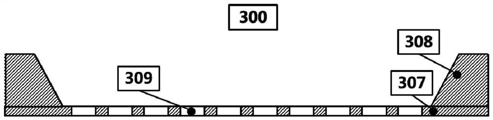
[0058] Such as image 3 As shown, the present embodiment provides a field emission cathode ultra-thin refractory metal grid 300, which includes: a grid substrate 307, including a grid through-hole array 309 in the central area of ​​the grid substrate 307; the grid The support ring 308 is located on the grid substrate 307, and the two are welded together; wherein, the material of the grid substrate 307 is refractory metal.

[0059] Exemplary, refractory metals suitable for the grid substrate 307 in this embodiment include but are not limited to tungsten, molybdenum, tantalum, etc., and molybdenum is preferred in this embodiment.

[0060] In this embodiment, the thickness of the grid substrate 307 ranges from 40 micrometers to 5 micrometers according to different frequency bands of millimeter wave and terahertz devices. Exemplary thicknesses include, but are not limited to, 35 microns to 5 microns, 35 microns to 10 microns, 35 microns to 15 microns, 35 microns to 20 microns, 30...

Embodiment 2

[0088] Repeat Example 1, the difference is that in step 2), the pattern of photoresist 304 formed by exposure and development is a square column, with a side length of 80 microns, and a distance of 10 microns between each column; in step 3), photoetching The silicon device layer 303 forms a silicon mold 305 pattern that is a square column, with a side length of 80 microns and a distance of 10 microns between each column. Other conditions remain unchanged. The result of the grid 300 obtained in this embodiment is similar to that of Example 1, the difference is that the grid The extremely transparent array hole 309 is a square hole array with a light transmittance of 80%.

Embodiment 3

[0090] Repeat Example 1, the difference is that in step 1), the thickness of the silicon device layer 303 is changed to 12 microns; in step 4), the thickness of the gate deposition layer 306 is changed to 13 microns; The layer 306 / silicon mold 305 mixed layer grinding thickness is changed to 11 microns, the polishing thickness is changed to 10 microns, and other conditions remain unchanged. The result of the grid 300 obtained in this embodiment is similar to that of Example 1, and the difference is the thickness of the grid substrate 307. to 10 microns.

[0091] The method of the present invention breaks through the limitation that the conventional laser processing or photolithographic etching method can only realize grids with a thickness exceeding 50 microns, and the UV-LIGA process can only make electroplating-related metal materials, and can realize any thickness within the range of 5-50 microns ( For example, the ultra-thin refractory metal grid of 5-20 microns), and the ...


PUM

PropertyMeasurementUnit
thicknessaaaaaaaaaa
thicknessaaaaaaaaaa
thicknessaaaaaaaaaa

Abstract

The invention discloses a field emission cathode ultra-thin refractory metal grid mesh which comprises a grid mesh substrate with a grid through hole array at the central area of the grid mesh substrate; and a grid mesh supporting ring which is positioned on the grid mesh substrate, wherein the grid mesh supporting ring and the grid mesh substrate are welded integrally, and the grid mesh substrateis made of refractory metal. The grid mesh has ultra-thin thickness, can be suitable for cold cathodes of millimeter wave and terahertz vacuum electronic devices, and realizes good comprehensive performance of the devices. The invention also provides a preparation method of the field emission cathode ultra-thin refractory metal grid mesh.

Description

technical field [0001] The invention relates to the field of vacuum microelectronics. More specifically, it relates to a field emission cathode ultra-thin refractory metal grid and a preparation method thereof. Background technique [0002] The field emission cathode does not require external heating energy and light energy. Only by applying a strong electric field to suppress the surface barrier of the cathode, the height and width of the barrier can be reduced, so that the electrons in the emitter can escape through the tunnel effect. Compared with traditional thermal emission cathodes, field emission cold cathodes compatible with microfabrication technology have the characteristics of low power consumption, small size, fast response speed, room temperature operation, and high current density, and are expected to be used in traditional vacuum electronic devices to achieve better performance . [0003] There are two main structural forms of the grid for extracting electro...

Claims


Application Information

Patent Timeline
Patent Type & Authority Applications(China)
IPC IPC(8): H01J1/304H01J9/02
CPCH01J1/304H01J9/025
Inventor 李兴辉韩攀阳杜婷姜琪杨金生蔡军冯进军
Owner NO 12 RES INST OF CETC
Why Eureka
Try Eureka