Trench power device and manufacturing method thereof

A technology for power devices and manufacturing methods, which is applied in semiconductor/solid-state device manufacturing, semiconductor devices, electrical components, etc., and can solve the problems of limited integration of lithography machines, high relative position requirements, and high lithography alignment requirements. , to achieve the effects of cost controllable, improved integration, and improved device efficiency

Pending Publication Date: 2021-02-19
ALPHA & OMEGA SEMICON LTD
View PDF6 Cites 2 Cited by
  • Summary
  • Abstract
  • Description
  • Claims
  • Application Information

AI Technical Summary

Problems solved by technology

This method has high requirements for photolithography alignment in the source trench photolithography process, which limits the reduction of cell density.
Moreover, due to the structural characteristics of trench p

Method used


Image

  • Trench power device and manufacturing method thereof
  • Trench power device and manufacturing method thereof
  • Trench power device and manufacturing method thereof

Examples


Example Embodiment

[0072]Example 1

[0073]A trench power device and a manufacturing method thereof, including the following steps:

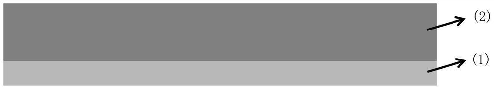
[0074]Step S1, such asfigure 1 As shown, an epitaxial layer 2 is grown on a silicon substrate 1, and the epitaxial layer 2 is grown by chemical weather deposition. The epitaxial layer 2 can be doped with trivalent element boron or pentavalent element arsenic and phosphorus according to the polarity of the device. In this embodiment, trivalent element boron can be doped. The epitaxial layer 2 can have a micron-level change in thickness or adopt a multilayer structure according to the working voltage.

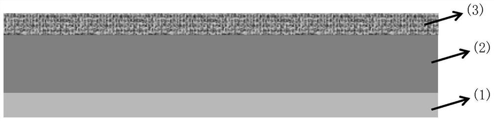
[0075]Step S2, such asfigure 2 As shown, the mask 3 used to form the trench is deposited next. The mask 3 may be a photoresist or a multilayer combined structure of photoresist and other insulator masks. Such as: silicon dioxide-silicon nitride-silicon dioxide. Silicon dioxide and silicon nitride are prepared by chemical weather deposition process; photoresist is spin-coated by ph...

Example Embodiment

[0097]Example 2

[0098]A trench power device and a manufacturing method thereof, including the following steps:

[0099]Step S1, such asfigure 1 As shown, an epitaxial layer 2 is grown on a silicon substrate 1, and the epitaxial layer 2 is grown by chemical weather deposition. The epitaxial layer 2 can be doped with trivalent element boron or pentavalent element arsenic and phosphorus according to the polarity of the device. In this embodiment, pentavalent element arsenic can be doped. The epitaxial layer 2 can have a micron-level change in thickness or adopt a multilayer structure according to the working voltage.

[0100]Step S2, such asfigure 2 As shown, the mask 3 used to form the trench is deposited next. The mask 3 may be a photoresist or a multilayer combined structure of photoresist and other insulator masks. Such as: silicon dioxide-silicon nitride-silicon dioxide. Silicon dioxide and silicon nitride are prepared by chemical weather deposition process; photoresist is spin-coated b...

Example Embodiment

[0122]Example 3

[0123]A trench power device and a manufacturing method thereof, including the following steps:

[0124]Step S1, such asfigure 1 As shown, an epitaxial layer 2 is grown on a silicon substrate 1, and the epitaxial layer 2 is grown by chemical weather deposition. The epitaxial layer 2 can be doped with trivalent element boron or pentavalent element arsenic and phosphorus according to the polarity of the device. In this embodiment, pentavalent element phosphorus is doped. The epitaxial layer 2 can have a micron-level change in thickness or adopt a multilayer structure according to the working voltage.

[0125]Step S2, such asfigure 2 As shown, the mask 3 used to form the trench is deposited next. The mask 3 may be a photoresist or a multilayer combined structure of photoresist and other insulator masks. Such as: silicon dioxide-silicon nitride-silicon dioxide. Silicon dioxide and silicon nitride are prepared by chemical weather deposition process; photoresist is spin-coated by ...


PUM

PropertyMeasurementUnit
Thicknessaaaaaaaaaa
Thicknessaaaaaaaaaa
Thicknessaaaaaaaaaa

Abstract

The invention discloses a trench power device and a manufacturing method thereof, and relates to the field of power device semiconductor manufacturing, and the method comprises the following steps: A,preparing a cellular structure; B, preparing a contact hole and a tungsten bolt; C, etching to form a circuit; and D, depositing a passivation layer, and etching the passivation layer. According to the invention, the process limitation on the relative positions of the gate trench and the source trench imposed by the process ability of a photoetching machine platform of a factory is overcome, andthe integration level is further improved. By manufacturing the gate trench and the source trench at the same time, the difficulty of the photoetching process is overcome, and the cost is controllabledue to the fact that a mask plate is not added. The cell density can be further reduced, the conduction resistance is reduced, and the device efficiency is improved.

Description

Technical field[0001]The present invention relates to the field of power device semiconductor manufacturing, in particular to a trench power device and a manufacturing method thereof.Background technique[0002]Due to the importance of environmental protection from all walks of life, power devices have become increasingly prominent in electronic power applications due to their energy-saving features. In particular, trench power devices are favored by market applications due to their low on-resistance and high integration.[0003]The Chinese invention patent with publication number CN102956481B provides a method for manufacturing trench-type power semiconductor devices with source trenches. First, at least two gate trenches are formed in the substrate; then, dielectrics are sequentially formed Layer and polysilicon structure in the gate trench; subsequently, at least one source trench is formed between two adjacent gate trenches; next, a dielectric layer and a second polysilicon structur...

Claims


Application Information

Patent Timeline
IPC IPC(8): H01L21/28H01L21/336H01L29/417H01L29/423H01L29/78
CPCH01L29/66666H01L29/7827H01L29/401H01L29/41741H01L29/41775H01L29/4236Y02B70/10H01L21/3065H01L21/3083H01L29/41766H01L29/456
Inventor 杨笠石亮
Owner ALPHA & OMEGA SEMICON LTD
Why Eureka
Try Eureka