
A Guard Ring for Gallium Nitride-Based Active Devices

An active device, GaN-based technology, applied in semiconductor devices, electric solid-state devices, semiconductor/solid-state device components, etc., can solve the problems of mutual interference of active devices, high power, and deterioration of chip product performance. The effect of reducing parasitic resistance

Active Publication Date: 2021-07-30
深圳市易星标技术有限公司
View PDF5 Cites 0 Cited by
  • Summary
  • Abstract
  • Description
  • Claims
  • Application Information

AI Technical Summary

Problems solved by technology

The frequency range of millimeter waves is 26.5-300GHz. GaN RF front-end chips designed in this frequency band often face the problem of mutual interference between active devices due to their high frequency and high power, which further causes problems such as deterioration of the performance of finished chips.

Method used


Image

  • A Guard Ring for Gallium Nitride-Based Active Devices
  • A Guard Ring for Gallium Nitride-Based Active Devices
  • A Guard Ring for Gallium Nitride-Based Active Devices

Examples


Embodiment Construction

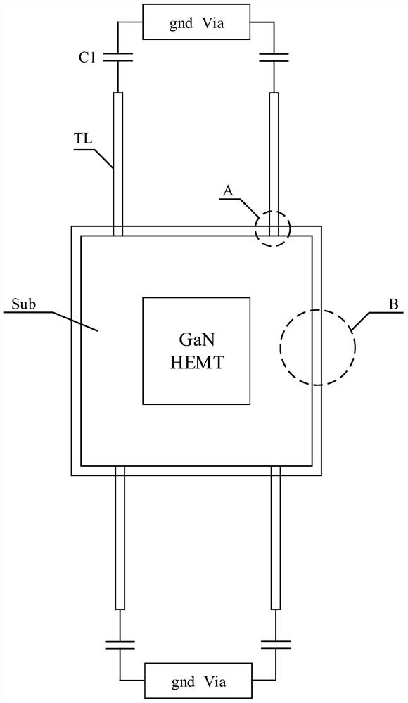
[0022] like Figure 1-Figure 2 As shown, the guard ring of a gallium nitride-based active device described in the present invention is arranged on the substrate of the chip, including an ohmic contact layer Oh-C that forms a closed ring, and a stacked layer arranged on the ohmic contact layer on the first metal layer Met1. The first metal layer is connected to the upper second metal layer through a vertical through hole, and the second metal layer is provided with a microstrip line, and the microstrip line is electrically connected to the ground via hole after being connected in series with a lumped capacitor. Active devices can be arranged in the space surrounded by the ohmic contact layer and the first metal layer. The active device in this embodiment takes GaN HEMT as an example.

[0023] The ohmic contact layer and the first metal layer form an absorbing ring for high-frequency noise, which can be the high-frequency noise that diffuses outward in the absorbing ring, and ...


PUM

PropertyMeasurementUnit
thicknessaaaaaaaaaa
thicknessaaaaaaaaaa
thicknessaaaaaaaaaa

Abstract

The invention discloses a protection ring of a gallium nitride-based active device, and relates to a new generation of information technology. The guard ring includes an ohmic contact layer arranged on the substrate to form a closed loop, and a first metal layer is stacked on the ohmic contact layer; the first metal layer is connected to the second metal layer above through a vertical through hole, The second metal layer is provided with a microstrip line, and the microstrip line is connected in series with the lumped capacitor and is electrically connected to the ground via. The advantage is that by adjusting the size of the lumped capacitor reasonably, the ground impedance of the guard ring can be minimized, and the high-frequency noise generated by the active devices in the ring can be effectively absorbed and exported to the reference ground plane. Simulation tests show that adding a guard ring can improve high-frequency noise isolation by more than 10dB. The disposition of the first metal layer can reduce the parasitic resistance of the ohmic contact layer.

Description

technical field [0001] The invention relates to a protection structure of a high-frequency chip, in particular to a protection ring of a gallium nitride-based active device. Background technique [0002] In the field of third-generation semiconductor integrated circuits, millimeter-wave radio frequency chips based on gallium nitride technology are one of the most important modules in 5G communication chips. Widely used in automotive radar, aircraft radar, precision guidance and satellite communication, etc. Gallium nitride HEMT is the most important active device in gallium nitride chips. Its characteristics of high withstand voltage, low noise and high electron mobility are very suitable for high-performance power amplifiers (PA), low-noise amplifiers (LNA) and RF switches. (SW) design. The frequency range of millimeter waves is 26.5-300 GHz. Due to the high frequency and high power of GaN RF front-end chips designed in this frequency band, they often face the problem of ...

Claims


Application Information

Patent Timeline
Patent Type & Authority Patents(China)
IPC IPC(8): H01L23/58H01L23/66H01L29/778
CPCH01L23/585H01L23/66H01L29/778H01L2223/6616H01L2223/6627
Inventor 邹宇陈志坚赖俊凯李斌
Owner 深圳市易星标技术有限公司
Learn More