Surface passivation structure for III-V group nitride device and device thereof

A nitride and device technology, which is applied in semiconductor devices, semiconductor/solid-state device manufacturing, electrical components, etc., can solve problems such as current density drop, devices cannot be completely turned on, and negative charges cannot be released in time

Active Publication Date: 2021-02-26
XIAMEN SANAN INTEGRATED CIRCUIT
View PDF5 Cites 1 Cited by
  • Summary
  • Abstract
  • Description
  • Claims
  • Application Information

AI Technical Summary

Problems solved by technology

When the gate voltage is applied to the device and the device is turned on, the channel under the gate is turned on, but the negative charges in the negative charge trap area of ​​the interface cannot be released in time, resulting in the incomplete conduction of the device, resulting in a decrease in current density and a decrease in output power. occur

Method used


Image

  • Surface passivation structure for III-V group nitride device and device thereof
  • Surface passivation structure for III-V group nitride device and device thereof
  • Surface passivation structure for III-V group nitride device and device thereof

Examples


Embodiment 1

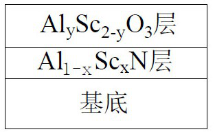
[0027] Such as figure 1As shown, a surface passivation structure for III-V nitride devices, including Al 0.2 sc 0.8 N layer and AlScO 3 layer, where Al 0.2 sc 0.8 The thickness of N layer is 1nm, AlScO 3 The thickness of the layer is 1 nm.

[0028] The specific production method is as follows: Step 1: Control the operating chamber of the atomic layer deposition system at 425°C, and after the substrate temperature is stable, inject trimethylaluminum (0.2s) and ammonia (0.5 s), trimethylaluminum (0.2s), triisopropylcyclopentadienyl scandium (2s), after 8 cycles, a 1.0nm thin layer of aluminum scandium nitride (Al 0.2 sc 0.8 N). Step 2: Cool down the operating chamber of the atomic layer deposition system and control it at 300°C, and after the substrate temperature is stable, pass in trimethylaluminum (0.2s), deionized water (0.5s), three Methyl aluminum (0.2s), triisopropylcyclopentadienyl scandium (2s), after 5 cycles, a 1.0nm thin layer of aluminum scandium oxide (AlS...

Embodiment 2

[0030] A surface passivation structure for III-V nitride devices, comprising Al 0.2 sc 0.8 N layer and AlScO 3 layer, where Al 0.2 sc 0.8 The thickness of N layer is 0.5nm, AlScO 3 The thickness of the layer is 2 nm.

[0031] The specific production method is as follows: Step 1: Control the operating chamber of the atomic layer deposition system at 425°C, and after the substrate temperature is stable, inject trimethylaluminum (0.2s) and ammonia (0.5 s), trimethylaluminum (0.2s), triisopropylcyclopentadienyl scandium (2s), after 8 cycles, a 1.0nm thin layer of aluminum scandium nitride (Al 0.2 sc 0.8 N). Step 2: Cool down the operating chamber of the atomic layer deposition system and control it at 300°C, and after the substrate temperature is stable, pass in trimethylaluminum (0.2s), deionized water (0.5s), three Methyl aluminum (0.2s), triisopropylcyclopentadienyl scandium (2s), after 10 cycles, a 2.0nm thin layer of aluminum scandium oxide (AlScO) can be deposited on...

Embodiment 3

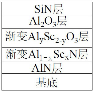
[0033] Such as figure 2 As shown, a surface passivation structure for III-V nitride devices, including AlN layer, Al 0.2 sc 0.8 N layer, Al 0.6 sc 0.4 N layer, Al 1.2 sc 0.8 o 3 layer, AlScO 3 layer. Among them, the thickness of AlN layer is 0.3nm, Al 0.2 sc 0.8 The thickness of N layer is 0.3nm, Al 0.6 sc 0.4 The thickness of N layer is 0.4nm, Al 1.2 sc 0.8 o 3 layer thickness of 0.5nm, AlScO 3 The thickness of the layer is 1nm, Al 2 o 3 The thickness of the layer is 0.5 nm.

[0034] In this example, Al 1-x sc x The N layer is specifically composed of Al 0.2 sc 0.8 N layer and Al 0.6 sc 0.4 N layers, the content of Al in each layer increases from bottom to top, and the content of Sc decreases from bottom to top. Al y sc 2-y o 3 Al 1.2 sc 0.8 o 3 layer and AlScO 3 Layers, the Al content in each layer decreases from bottom to top, and the Sc content increases from bottom to top. Gradient Al 1-x sc x N layer and graded Al y sc 2-y o 3 The la...


PUM

PropertyMeasurementUnit
thicknessaaaaaaaaaa
thicknessaaaaaaaaaa
thicknessaaaaaaaaaa

Abstract

The invention discloses a surface passivation structure for a III-V group nitride device and a device thereof. The surface passivation structure comprises an Al1-xScxN layer and an AlySc2-yO3 layer, the Al1-xScxN layer and the AlySc2-yO3 layer are located on a III-V nitride substrate, the Al1-xScxN layer and the AlySc2-yO3 layer are sequentially stacked from bottom to top, the thickness of the Al1-xScxN layer is 0.5-10 nm, x is larger than 0 and equal to or smaller than 1, the thickness of the AlySc2-yO3 layer is 1-20nm, y is more than or equal to 0 and less than 2, and the thickness of the Al1-xScxN layer is less than or equal to the thickness of the AlySc2-yO3 layer. Generation of an interface state can be further reduced, the risk of current collapse of the device is reduced, and the reliability of the device is improved.

Description

technical field [0001] The invention relates to the technical field of semiconductors, in particular to a surface passivation structure for III-V group nitride devices and devices thereof. Background technique [0002] Electronic power technology plays an important role in the production and life of modern humans. From household appliances in daily life to industrial production, electrical transportation and new energy technologies, power electronic devices are everywhere. Among them, III-V nitride electronic power devices represented by gallium nitride materials have been widely used. Gallium Nitride (GaN), as the third-generation wide-bandgap semiconductor material, has outstanding advantages in characteristics compared with traditional silicon (Si)-based semiconductor materials. Due to the large band gap and high thermal conductivity, GaN devices can carry higher energy density and higher reliability; the larger band gap and breakdown electric field reduce the on-resista...

Claims


Application Information

Patent Timeline
Patent Type & Authority Applications(China)
IPC IPC(8): H01L29/06H01L29/20H01L29/40H01L29/778H01L21/02
CPCH01L29/0611H01L29/2003H01L29/408H01L29/778H01L21/02178H01L21/022H01L21/0228H01L21/02164H01L21/0217H01L21/02274
Inventor 郭德霄林志东何俊蕾王立阁汪晓媛赵杰刘成叶念慈
Owner XIAMEN SANAN INTEGRATED CIRCUIT
Why Eureka
Try Eureka