Nitride semiconductor device and production process thereof

a technology of nitride semiconductor and production process, which is applied in the direction of semiconductor devices, basic electric elements, electrical appliances, etc., can solve the problems of insufficient realization of high breakdown voltage of wide band gap material, affecting the breakdown voltage of conventional nitride semiconductor devices, and fluctuating surface potential, so as to reduce gate leakage current, reduce the effect of high insulating property and reduce the leakage curren

Active Publication Date: 2005-06-02
NEW JAPAN RADIO CORP
View PDF4 Cites 1 Cited by
  • Summary
  • Abstract
  • Description
  • Claims
  • Application Information

AI Technical Summary

Benefits of technology

[0004] However, the breakdown voltage of a conventional nitride semiconductor device is affected by the Schottky property which is formed by bringing a gate metal in contact with the nitride semiconductor layer. High gate leakage current is observed for the Schottky property of the gate metal which is generally formed on a nitride semiconductor layer, for example, an aluminum gallium nitride (AlGaN) layer and a gallium nitride (GaN) layer. There has been a problem that this becomes a trigger for impact ionization, lowers the OFF-state breakdown voltage (the drain breakdown voltage at a condition in which FET is OFF) which is the important parameter of a nitride semiconductor device being a high output power, smaller than a value expected, and the characteristic of the high breakdown voltage of a wide band gap material cannot be adequately realized. On the other hand, there have been problems that surface potential is fluctuated and the frequency dispersion of current-voltage characteristic is also generated in a semiconductor device in which the gate electrode was formed on the nitride semiconductor layer such as an aluminum gallium nitride (AlGaN) layer and a gallium nitride (GaN) layer, by electrons trapped in the surface states of the nitride semiconductor layer. The purpose of the present invention is to provide a nitride semiconductor device which reduces greatly the leakage current in the Schottky property of the control electrode (gate electrode) which is formed on the nitride semiconductor device, realizes the high breakdown voltage by suppressing the impact ionization in the nitride semiconductor device and can suppress the frequency dispersion and a process for producing thereof.
[0017] The nitride semiconductor device according to the invention of the present application is a structure in which the control electrode is making contact with a nitride semiconductor layer not containing at least aluminum, and leakage current can be reduced by making the nitride semiconductor layer be the crystallinity with minute grains with high insulating property. When the control electrode of the present invention was set as the gate electrode such as FET or HEMT, gate leakage current is reduced. Further, the high breakdown voltage can be realized by suppressing the impact ionization at the channel. Since the structure in which the nitride semiconductor layer consisting of the crystallinity with minute grains with high insulating property is provided between the gate electrode and the drain electrode is made, electrons which are trapped in the surface states between the gate electrode and the drain electrode are suppressed or current collapse phenomenon is suppressed by reduction of the surface states density and high frequency characteristics are also improved.
[0018] Further, since the screening effect for carriers trapped in the surface states is revealed by forming the p-type nitride semiconductor region between the gate electrode and the drain electrode, the frequency dispersion of current-voltage characteristic caused by fluctuation of surface potential can be suppressed.
[0019] Further, since the process for producing the nitride semiconductor device according to the present invention can form a nitride semiconductor device with a desired structure by control of the temperature of epitaxial growth by the production steps of a usual nitride semiconductor device and only by control of the ion implantation method, the controllability of the production steps is superior and the nitride semiconductor device superior in characteristics can be produced in good yield.

Problems solved by technology

However, the breakdown voltage of a conventional nitride semiconductor device is affected by the Schottky property which is formed by bringing a gate metal in contact with the nitride semiconductor layer.
There has been a problem that this becomes a trigger for impact ionization, lowers the OFF-state breakdown voltage (the drain breakdown voltage at a condition in which FET is OFF) which is the important parameter of a nitride semiconductor device being a high output power, smaller than a value expected, and the characteristic of the high breakdown voltage of a wide band gap material cannot be adequately realized.
On the other hand, there have been problems that surface potential is fluctuated and the frequency dispersion of current-voltage characteristic is also generated in a semiconductor device in which the gate electrode was formed on the nitride semiconductor layer such as an aluminum gallium nitride (AlGaN) layer and a gallium nitride (GaN) layer, by electrons trapped in the surface states of the nitride semiconductor layer.

Method used


Image

  • Nitride semiconductor device and production process thereof
  • Nitride semiconductor device and production process thereof
  • Nitride semiconductor device and production process thereof

Examples


embodiment 1

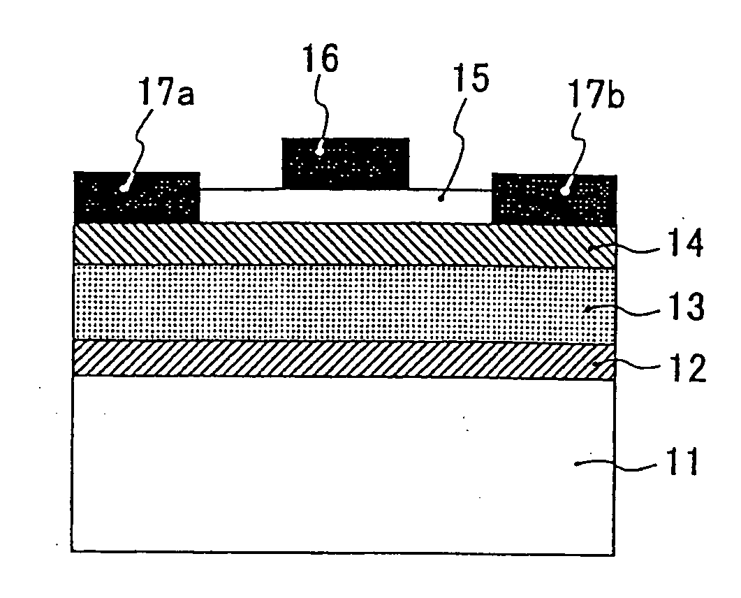
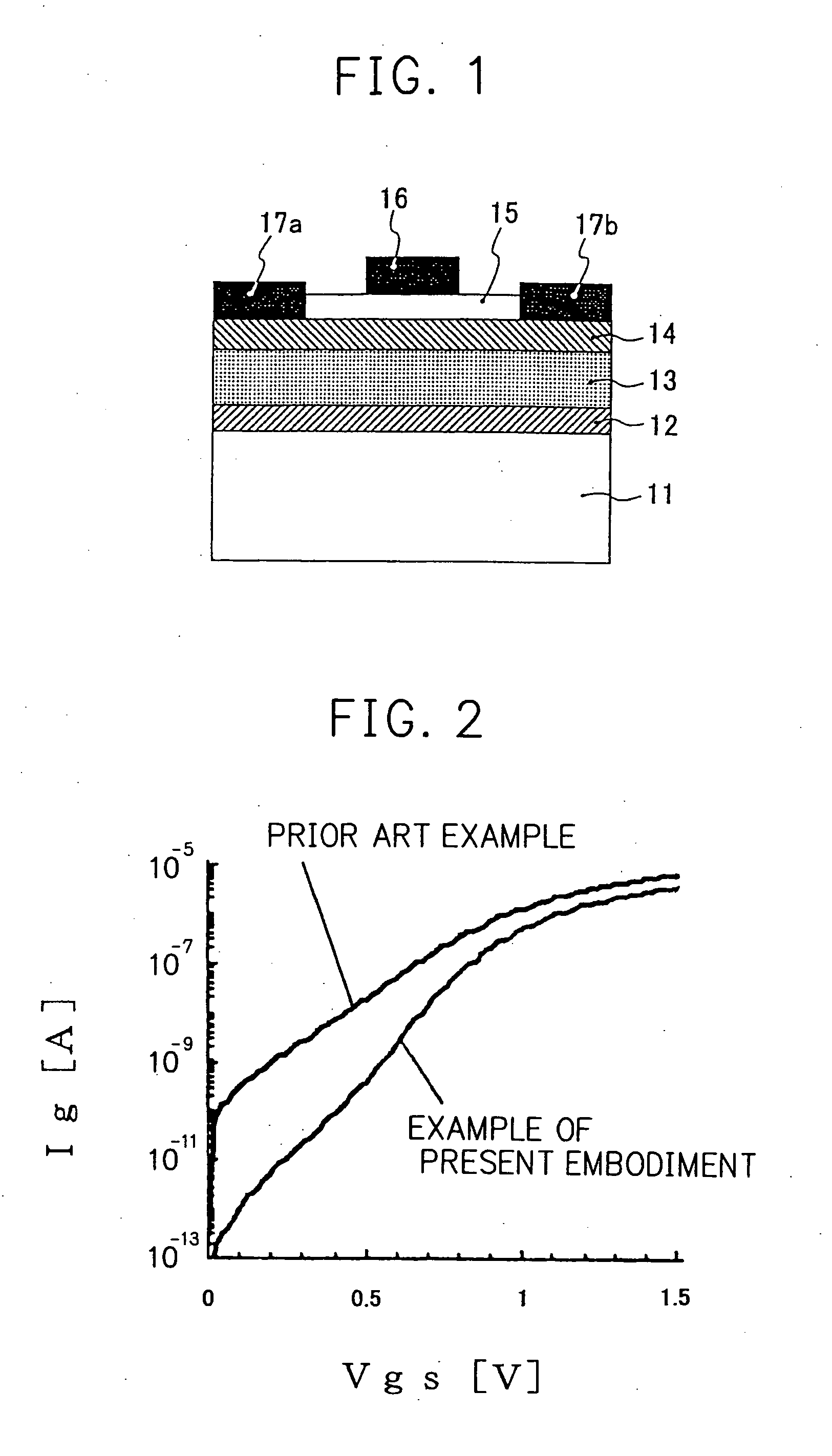
[0031] Firstly, the nitride semiconductor device of the present invention is specifically illustrated referring to HEMT which is the III-V Group nitride semiconductor device as an example. FIG. 1 is the cross-section view of HEMT which is the III-V Group nitride semiconductor device which is the first Embodiment of the present invention. As shown in FIG. 1, a buffer layer 12 consisting of aluminum nitride (AlN) with a thickness of about 100 nm, a channel layer 13 consisting of non-doped gallium nitride (GaN) with a thickness of 2 μm having a smaller energy band gap than that of a charge supply layer described later, a charge supply layer 14 consisting of n-type aluminum gallium nitride (AlGaN) with a thickness of 15 nm which forms the two dimensional electron gas being careers at an interface with the channel layer 13 and a Schottky layer 15 consisting of non-doped gallium nitride (GaN) with a thickness of 10 nm having the cristallinity with minute grains were formed by deposition o...

embodiment 2

[0034] Then, the second Embodiment is illustrated. FIG. 5 is the cross-section view of HEMT which is the III-V Group nitride semiconductor device which is the second Embodiment of the present invention. In like manner as the first Embodiment as shown in FIG. 1, a buffer layer 12 consisting of aluminum nitride (AlN) with a thickness of about 100 nm, a channel layer 13 consisting of non-doped gallium nitride (GaN) with a thickness of 2 μm, a charge supply layer 14 consisting of n-type aluminum gallium nitride (AlGaN) with a thickness of 15 nm which forms the two dimensional electron gas being careers at an interface with the channel layer 13 and a Schottky layer 15 consisting of non-doped gallium nitride (GaN) with a thickness of 10 nm having the crystallinity with minute grains are formed by deposition on a substrate 11 consisting of silicon carbide (SiC). The gate electrode 16 consisting of a laminate of nickel (Ni) / gold (Au) and the like is formed on the Schottky layer 15 and the S...

embodiment 3

[0036]FIG. 6 is the cross-section view of HEMT which is the III-V Group nitride semiconductor device which is the third Embodiment of the present invention. In like manner as the first Embodiment as shown in FIG. 1, a buffer layer 12 consisting of aluminum nitride (AlN) with a thickness of about 100 nm, a channel layer 13 consisting of non-doped gallium nitride (GaN) with a thickness of 2 μm, a charge supply layer 14 consisting of n-type aluminum gallium nitride (AlGaN) with a thickness of 15 nm which forms the two dimensional electron gas being careers at an interface with the channel layer 13 and a Schottky layer 15 consisting of non-doped gallium nitride (GaN) with a thickness of 10 nm having the crystallinity with minute grains are formed by deposition on a substrate 11 consisting of silicon carbide (SiC). The gate electrode 16 consisting of a laminate of nickel (Ni) / gold (Au) and the like is formed on the Schottky layer 15 and the Schottky contact is made with the Schottky laye...


PUM

PropertyMeasurementUnit
thicknessaaaaaaaaaa
thicknessaaaaaaaaaa
thicknessaaaaaaaaaa

Abstract

A nitride semiconductor device, which includes a III-V Group nitride semiconductor layer being composed of a III Group element consisting of at least one of a group containing of gallium, aluminum, boron and indium and V Group element consisting of at least nitrogen among a group consisting of nitrogen, phosphorus and arsenic, including a first nitride semiconductor layer including the III-V Group nitride semiconductor layer being deposited on a substrate, a second nitride semiconductor layer including the III-V Group nitride semiconductor layer being deposited on the first nitride semiconductor and not containing aluminum and a control electrode making Schottky contact with the second nitride semiconductor layer wherein the second nitride semiconductor layer includes a film whose film forming temperature is lower than the first nitride semiconductor layer.

Description

BACKGROUND OF THE INVENTION [0001] The present invention relates to a nitride semiconductor device using nitride semiconductors for active layers and a process for producing thereof, and specifically, relates to a nitride semiconductor device which is making Schottky contact with a semiconductor device such as a High Electron Mobility Transistor (HEMT) and a Field Effect Transistor (FET) and a process for producing thereof. [0002]FIG. 10 shows the cross-section view of a semiconductor device comprising a conventional III-V Group nitride semiconductor. The semiconductor device shown in FIG. 10 shows a so-called HEMT structure and it is a structure in which a buffer layer 102 consisting of gallium nitride (GaN), a channel layer 103 consisting of gallium nitride, a charge supply layer 104 consisting of n-type aluminum gallium nitride (AlGaN) and a Schottky layer 105 consisting of non-doped aluminum gallium nitride were deposited in order on a substrate 101 consisting of a sapphire subs...

Claims


Application Information

Patent Timeline
Patent Type & Authority Applications(United States)
IPC IPC(8): H01L21/28H01L21/205H01L21/318H01L21/335H01L21/338H01L29/20H01L29/417H01L29/778H01L29/812
CPCH01L29/2003H01L29/7787H01L29/66462H01L29/0619
Inventor NAKAGAWA, ATSUSHI
Owner NEW JAPAN RADIO CORP
Why Eureka
Try Eureka