Preparation method of heterojunction photoelectric detector based on single-walled carbon nanotube film

A technology of single-wall carbon nanotubes and photodetectors, applied in the field of photodetectors, can solve the problems of high dark current, poor detection performance, high cost, etc., and achieve the effects of fast response, simple structure and low cost

Pending Publication Date: 2021-02-26
INST OF METAL RESEARCH - CHINESE ACAD OF SCI
View PDF3 Cites 1 Cited by
  • Summary
  • Abstract
  • Description
  • Claims
  • Application Information

AI Technical Summary

Problems solved by technology

A single-walled carbon nanotube film with high photoelectric performance was prepared by floating catalyst chemical vapor deposition, which formed a heterojunction with an N-type silicon substrate, and a photodetector was prepared to solve the poor detection performance of traditional photodetectors at room temperature and atmospheric environment , high cost and other issues; at the same time, by preparing an induced oxide layer, the problem of excessive dark current of the device is solved to obtain a photodetector with high detectability and high stability

Method used


Image

  • Preparation method of heterojunction photoelectric detector based on single-walled carbon nanotube film
  • Preparation method of heterojunction photoelectric detector based on single-walled carbon nanotube film
  • Preparation method of heterojunction photoelectric detector based on single-walled carbon nanotube film

Examples


Embodiment 1

[0035] In this embodiment, the preparation method of a heterojunction photodetector based on a single-walled carbon nanotube film includes the following steps:

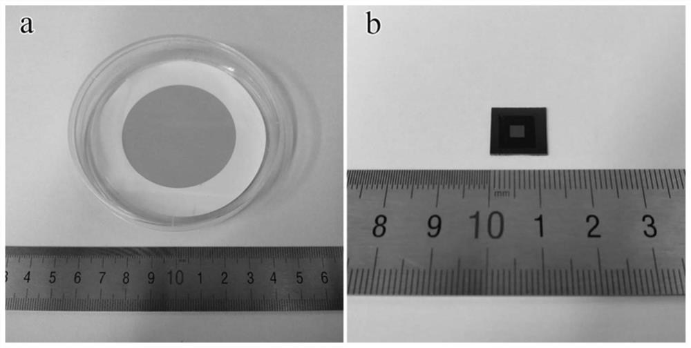
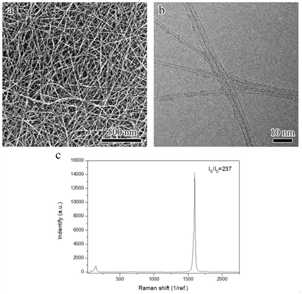
[0036] Step 1. Prepare a high-performance single-walled carbon nanotube film by floating catalyst chemical vapor deposition, grow single-walled carbon nanotubes under optimized conditions, and adjust the collection time to obtain a light transmittance range of 85% and a surface resistance of 110Ω / The single-walled carbon nanotube film of (sheet resistance), the single-walled carbon nanotube film deposited on the microporous membrane (in this embodiment, using a water-based microporous membrane with a pore size of 0.45 μm) is cut into a suitable size .

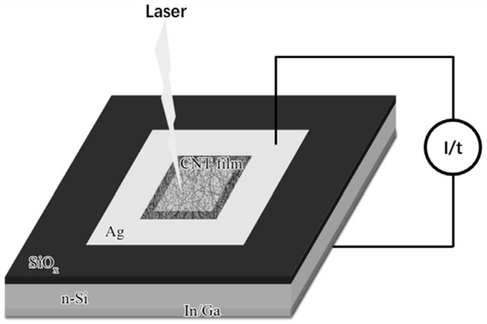
[0037] Step 2. Cut out an N-type silicon wafer with an area of ​​1.2cm×1.2cm and a thickness of 400μm (resistivity 0.05~0.2Ω·cm, with a silicon oxide layer with a thickness of 300nm), and first stick insulating tape on the silicon substrate On the upper surface, use ...

Embodiment 2

[0042] In this embodiment, the preparation method of a heterojunction photodetector based on a single-walled carbon nanotube film includes the following steps:

[0043] Step 1. Prepare a high-performance single-walled carbon nanotube film by floating catalyst chemical vapor deposition, grow single-walled carbon nanotubes under optimized conditions, and adjust the collection time to obtain a light transmittance range of 92% and a surface resistance of 500Ω / The single-walled carbon nanotube film of (sheet resistance), the single-walled carbon nanotube film deposited on the microporous membrane (in this embodiment, using a water-based microporous membrane with a pore size of 0.45 μm) is cut into a suitable size .

[0044] Step 2. Cut out an N-type silicon wafer with an area of ​​1.2cm×1.2cm and a thickness of 400μm (resistivity 0.05~0.2Ω·cm, with a silicon oxide layer with a thickness of 300nm), and first stick insulating tape on the silicon substrate On the upper surface, use ...

Embodiment 3

[0049] In this embodiment, the preparation method of a heterojunction photodetector based on a single-walled carbon nanotube film includes the following steps:

[0050] Step 1. Prepare a high-performance single-walled carbon nanotube film by floating catalyst chemical vapor deposition, grow single-walled carbon nanotubes under optimized conditions, and adjust the collection time to obtain a light transmittance range of 70% and a surface resistance of 60Ω / The single-walled carbon nanotube film of (sheet resistance), the single-walled carbon nanotube film deposited on the microporous membrane (in this embodiment, using a water-based microporous membrane with a pore size of 0.45 μm) is cut into a suitable size .

[0051] Step 2. Cut out an N-type silicon wafer with an area of ​​1.2cm×1.2cm and a thickness of 400μm (resistivity 0.05~0.2Ω·cm, with a silicon oxide layer with a thickness of 300nm), and first stick insulating tape on the silicon substrate On the upper surface, use a...


PUM

PropertyMeasurementUnit
diameteraaaaaaaaaa
thicknessaaaaaaaaaa
thicknessaaaaaaaaaa

Abstract

The invention relates to the field of photoelectric detectors, in particular to a preparation method of a heterojunction photoelectric detector based on a single-walled carbon nanotube film. The preparation method comprises the following steps: firstly, preparing a high-performance flexible single-walled carbon nanotube film by utilizing a floating catalyst chemical vapor deposition method, and cutting the single-walled carbon nanotube film deposited on a microporous filter membrane into a proper size; placing the single-walled carbon nanotube thin film on the upper surface of a silicon substrate with a preset window, enabling the single-walled carbon nanotube thin film to be in close contact with the silicon substrate, removing the filter membrane, and then placing the single-walled carbon nanotube thin film in an air environment for heat treatment so as to prepare an induced oxide layer with a thickness of several nanometers at the window; and then preparing an upper electrode (elargol) and a lower electrode (indium gallium alloy) to obtain the photoelectric detector. The heterojunction photoelectric detector is simple in structure and convenient in preparation process, and the constructed photoelectric detector has excellent photoelectric detection performance and stability.

Description

technical field [0001] The invention relates to the field of photodetectors, in particular to a method for preparing a heterojunction photodetector based on a single-walled carbon nanotube film. Background technique [0002] With the rapid development of the information industry and the massive increase in data, technologies such as information processing, computing, transmission, storage, and energy consumption control are facing unprecedented challenges. Light is one of the important carriers of information. Photon transmission has the advantages of high speed, low power consumption and strong anti-interference ability. Therefore, combining microelectronics and optoelectronics technology to realize optoelectronic integration has become an important development trend of the information industry. Photodetectors are important components in optical communication and optoelectronic integration. Their working principle is that photodetecting materials absorb incident photons and...

Claims


Application Information

Patent Timeline
Patent Type & Authority Applications(China)
IPC IPC(8): H01L51/48H01L51/42H01L51/46
CPCH10K85/221H10K30/10H10K2102/00Y02E10/549Y02P70/50
Inventor 侯鹏翔赵毅明胡显刚刘畅
Owner INST OF METAL RESEARCH - CHINESE ACAD OF SCI
Why Eureka
Try Eureka