Method for eliminating diffraction and interference caused by light passing through photomask
A photomask and light elimination technology, applied in the field of optical imaging, can solve problems such as distortion of lithographic imaging results, uneven exposure patterns, light diffraction and interference, etc., and achieve simple structure, good illumination uniformity, and light source utilization. high effect
- Summary
- Abstract
- Description
- Claims
- Application Information
AI Technical Summary
Problems solved by technology
Method used
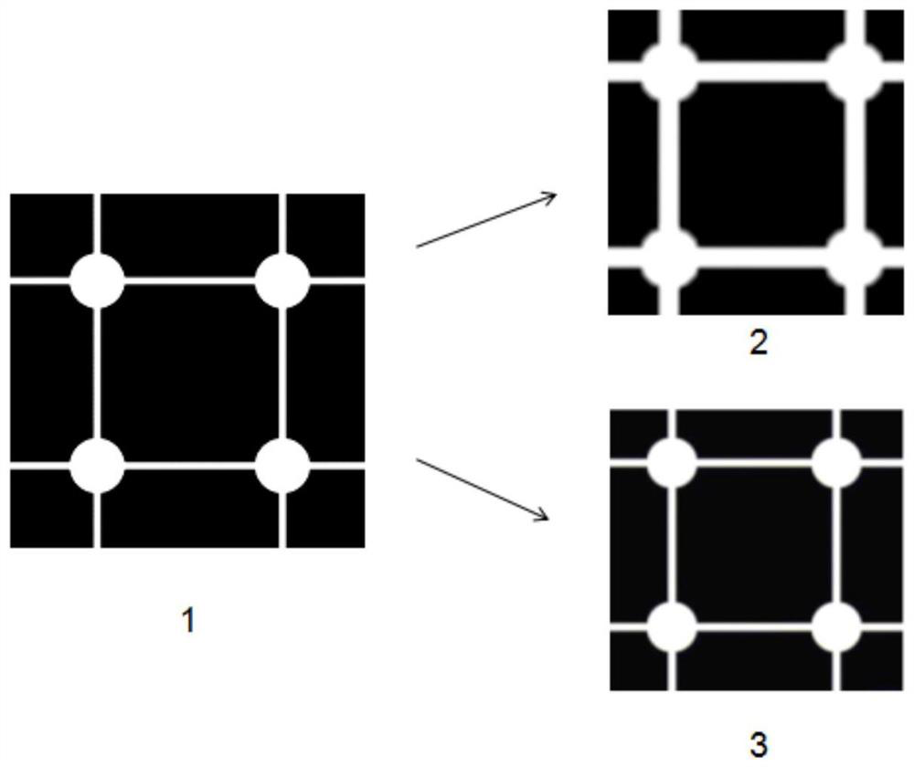
Image


Examples
Embodiment 1
[0023] EXAMPLIC A: This embodiment is used to eliminate the error of the exposure pattern during the exposure of the photolithography, exhibiting this method to eliminate the effect of diffraction and interference through the photomask, including the following steps:
[0024] Step 1: figure 1 The point source array is set in the lightning machine device, and the point light array is linearly arranged from squares of 9 sets of point light source according to 3 * 3, each set of point light sources consists of a square linear arrangement of nine LED point lights according to 3 * 3;
[0025] Step 2: In the point source array, the point light source of each group of point light source is mixed with a point of 380 nm, and the balance is a point light source of the wavelength of 365 nm;
[0026] Step 3: figure 2 As shown, 10 power controllers are set, 9 of which controls the point light sources of 365 nm wavelengths in each group of point light sources, and the other controller control...
Embodiment 2
[0029] Embodiment 2: This embodiment is for eliminating light by a method of diffuse and interference by a photomask as an example, exhibiting a specific process of eliminating the microena imaging graphic error caused by light winding and interference, including the following steps:
[0030] Step 1: Figure 4 In the photolithography device, the point source array is provided, and the point light source array is arranged by the 7-set point source according to the center symmetrical nominal shape, each set of point light sources consists of a square linear arrangement of 9 LED point light from 3 * 3;
[0031] Step 2: In the point light source array, mix the central point source group, 9 wavelengths of 380 nm, and 6 sets of point light source groups are points of 365 nm;
[0032] Step 3: Figure 5 As shown, seven power controllers are provided, wherein 6 controllers respectively control the 6-group wavelength 365 nm point light source group, another point light source group of wavele...
PUM
 Abstract
Description
Claims
Application Information
 - R&D
- Intellectual Property
- Life Sciences
- Materials
- Tech Scout
- Unparalleled Data Quality
- Higher Quality Content
- 60% Fewer Hallucinations
Browse by: Latest US Patents, China's latest patents, Technical Efficacy Thesaurus, Application Domain, Technology Topic, Popular Technical Reports.
© 2025 PatSnap. All rights reserved.Legal|Privacy policy|Modern Slavery Act Transparency Statement|Sitemap|About US| Contact US: help@patsnap.com