Thin film patterning process method, composite thin film and electronic component
A process method and thin-film graphic technology, which is applied in the manufacture of electrical components, piezoelectric/electrostrictive/magnetostrictive devices, semiconductor/solid-state devices, etc. Noise ratio, chirp, coupling efficiency and other issues to achieve the effect of reducing the difficulty of etching and increasing the etching rate
- Summary
- Abstract
- Description
- Claims
- Application Information
AI Technical Summary
Problems solved by technology
Method used
Image

Examples
Embodiment 1
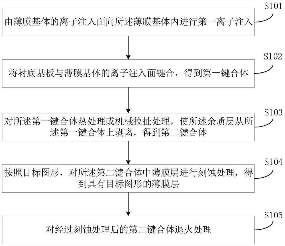
[0033] refer to figure 1 , the embodiment of the present application provides a film patterning process method, including the following steps:
[0034] Step 101, performing the first ion implantation from the ion implantation of the film matrix to the interior of the film matrix, forming a film layer, a separation layer and a residual layer in the film matrix.
[0035] The thin film substrate refers to a base material with a certain thickness, which is used to prepare the thin film layer, that is, a wafer with a certain thickness. The film substrate can be any material with optoelectronic or piezoelectric properties, such as lithium niobate, lithium tantalate, gallium arsenide, silicon, ceramic, lithium tetraborate, gallium arsenide, potassium titanyl phosphate, rubidium titanyl phosphate, or quartz and other materials, which are not limited in this application.
[0036] The embodiment of the present application does not specifically limit the first ion implantation method, ...
Embodiment 2
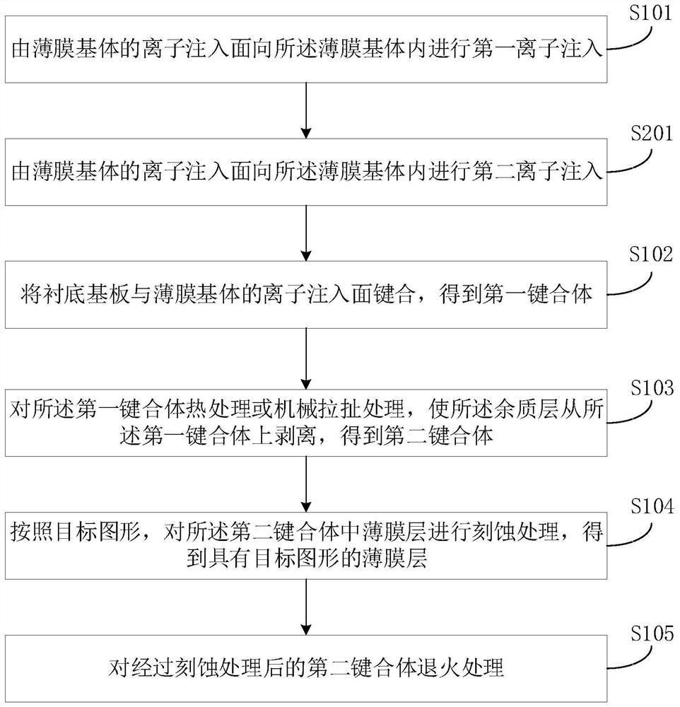
[0060] refer to figure 2 , the second embodiment of the present application is basically similar to the above-mentioned first embodiment, the difference is that, between the above-mentioned step 101 and step 102, the second embodiment of the present application adds the ion implantation of the thin-film substrate to the inside of the thin-film substrate. The step of two ion implantation is specifically as follows step 201:
[0061] Step 201, performing a second ion implantation from the ion implantation of the film matrix into the film matrix, the mass of implanted ions in the second ion implantation is greater than the mass of implanted ions in the first ion implantation, and the second ion implantation The implantation depth of the implantation is greater than the implantation depth of the first ion implantation.
[0062] Compared with the first ion implantation, the implanted ions of the second ion implantation adopt heavy ions, that is, the mass of the implanted ions of ...
Embodiment 3
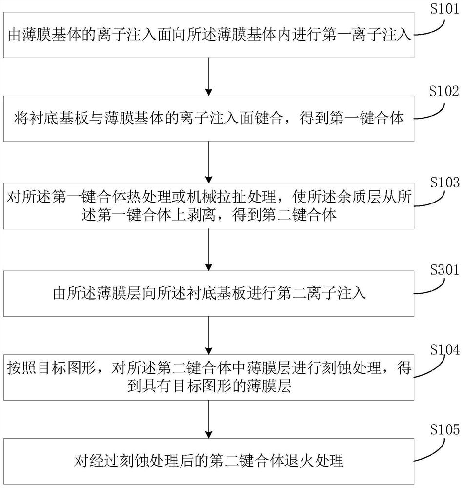
[0066] refer to image 3 , the third embodiment of the present application is basically similar to the first embodiment above, the difference is that, between the above step 103 and step 104, the third embodiment of the present application adds the second step from the thin film layer to the base substrate Ion implantation, specifically step 301 as follows:
[0067] Step 301: Perform a second ion implantation from the thin film layer to the base substrate, the implanted ion mass of the second ion implantation is greater than the implanted ion mass of the first ion implantation, and the second ion implantation The implantation depth is greater than the implantation depth of the first ion implantation.
[0068] The second bonded body prepared in step 103 includes a base substrate and a thin film layer stacked on the base substrate. In order to further increase the etching rate, a second ion implantation is performed from the thin film layer to the base substrate , wherein, for...
PUM
 Abstract
Description
Claims
Application Information
 - R&D Engineer
- R&D Manager
- IP Professional
- Industry Leading Data Capabilities
- Powerful AI technology
- Patent DNA Extraction
Browse by: Latest US Patents, China's latest patents, Technical Efficacy Thesaurus, Application Domain, Technology Topic.
© 2024 PatSnap. All rights reserved.Legal|Privacy policy|Modern Slavery Act Transparency Statement|Sitemap