LED epitaxial growth method

An epitaxial growth and reaction cavity technology, applied in the directions of crystal growth, single crystal growth, single crystal growth, etc., can solve the problems of low quantum well radiation recombination efficiency and low quantum well growth quality.

Pending Publication Date: 2021-04-20
XIANGNENG HUALEI OPTOELECTRONICS
View PDF0 Cites 4 Cited by
  • Summary
  • Abstract
  • Description
  • Claims
  • Application Information

AI Technical Summary

Problems solved by technology

[0005] The invention solves the problems of low quantum well growth quality and low quantum well radiation recombination efficiency existing in th

Method used


Image

  • LED epitaxial growth method
  • LED epitaxial growth method
  • LED epitaxial growth method

Examples


Embodiment 1

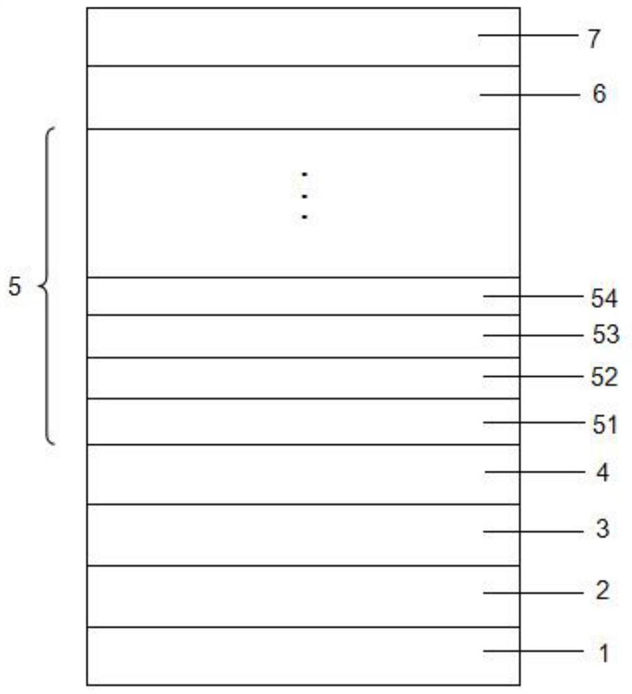
[0042]This embodiment employs the LED epitaxial growth method provided by the present invention, using MOCVD to grow GaN-based LED epitaxial sheet, using high purity H2High purity N2High purity H2High purity N2Mixed gas as carrier gas, high purity NH3Examples of N-source, metal organic source trimethyl gallium (TMGA) as gallium source, trimethyl indium (Tmin) as indium sources, N-type dopants are silane (SiH4), Trimethyl aluminum (TmAl) as aluminum sources, p-type dopants are fermented magnesium (CP2Mg), the reaction pressure between 70 mbar to 600 mbar. The specific growth mode is as follows (please refer to the epitaxial structurefigure 1 ):

[0043]LED epitaxial growth method, in turn, in turn, to process sapphire substrate 1, grow low temperature GaN buffer layer 2, growing non-doped GaN layer 3, GaN GaN layer 4, grown doped Si, growing multi-quantum well layer 5, growth AlGaN electronics The barrier layer 6, the p-type GaN layer 7 that grows doped Mg, cooling cooling; wherein

[0044...

Embodiment 2

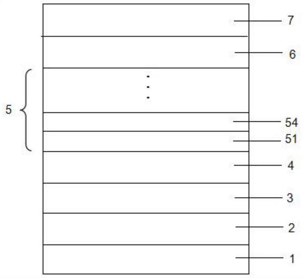
[0075]The above-mentioned embodiment is provided below, that is, the growth method of the traditional LED epitaxial structure (please refer to the extension structurefigure 2).

[0076]Step 1: In the temperature of 1000-1100 ° C, the reaction chamber pressure is 100-300 mbar, and the h of 100-130 l / min2Under the conditions, the sapphire substrate was processed for 5-10 minutes.

[0077]Step 2: Growth of the low temperature GaN buffer layer and form an irregular island in the low temperature GaN buffer layer 2.

[0078]Specifically, the step 2 is further:

[0079]At temperatures of 500-600 ° C, the reaction chamber pressure is 300-600 mbar, and the NH of 10000-20000sccm is passed.3, 50-100sccm TMGA, 100-130L / min H2Under the conditions, the low temperature GaN buffer layer 2 is grown on the sapphire substrate 1, and the thickness of the low temperature GaN buffer layer 2 is 20-40 nm;

[0080]At a temperature of 1000-1100 ° C, the reaction chamber pressure is 300-600 mbar, and the NH of 30000-400...


PUM

PropertyMeasurementUnit
Thicknessaaaaaaaaaa

Abstract

The invention discloses an LED epitaxial growth method, which sequentially comprises the steps of processing a substrate, growing a low-temperature GaN buffer layer, growing a non-doped GaN layer, growing a Si-doped N-type GaN layer, growing a multi-quantum well layer, growing an AlGaN electronic barrier layer, growing a Mg-doped P-type GaN layer, and cooling. Wherein the growth of the multi-quantum well layer sequentially comprises the steps of In-doped pretreatment, InGaN well layer growth, Ga2O3 pre-growth, Ga2O3 layer growth, annealing treatment, GaN gradient layer growth and GaN barrier layer growth. According to the method, the problems of low quantum well growth quality and low quantum well radiation recombination efficiency in the existing LED epitaxial growth method are solved, so that the luminous efficiency of the LED is improved.

Description

Technical field[0001]The present invention belongs to the field of LED technology, and more particularly to an LED epitaxial growth method.Background technique[0002]Light-Emitting Diode, LEDs are semiconductor electronic devices that convert electrical energy into light energy. When the LED is currently flowing, the electrons in the LEDs are monochromatic light from the holes in their multi-quantum wells. As an efficient, environmentally friendly, green new solid-state illumination source, LED source has the advantages of low voltage, low energy, small size, light weight, long life, high reliability and colorful color. At present, the size of the domestic production LED is gradually expanding, but the LED still has low luminous efficiency, affecting the energy saving effect of the LED.[0003]At present, the LED epitaxial inGan / GaN multi-quantum well quality prepared by the growth method of the existing LED multi-quantum well is low, and the radiation efficiency of the multi-quantum...

Claims


Application Information

Patent Timeline
IPC IPC(8): H01L33/00H01L33/06H01L33/12H01L33/14C30B25/00C30B25/02C30B29/16C30B29/40C30B31/06C30B33/02
Inventor 徐平夏玺华
Owner XIANGNENG HUALEI OPTOELECTRONICS
Why Eureka
Try Eureka