Method for processing core layer of arbitrary-layer interconnected high-density circuit board

A technology of arbitrary layer interconnection and processing method, applied in the direction of printed circuit, printed circuit manufacturing, and the formation of electrical connection of printed components, which can solve the problems of inability to directly manufacture ultra-fine circuits and affect product quality, saving resources and reducing production. cost effect

Active Publication Date: 2021-04-30
麦德美科技(苏州)有限公司
View PDF11 Cites 4 Cited by
  • Summary
  • Abstract
  • Description
  • Claims
  • Application Information

AI Technical Summary

Problems solved by technology

[0007] (2) The thickness of the dielectric layer used in the core layer is usually 65μm or 75μm, plus the upper copper, the size of the blind hole is 100x70μm or 100x80μm, and the ordinary electroplating hole filling potion is used for hole filling electroplating, and the blind hole needs to be electroplated for 18μm. , the surface copper after electroplating has reached more than 25μm, and it is impossible to directly make ultra-fine lines;
[0008] (3) After the electroplating and hole filling is completed, it needs to be baked at high temperature for several hours to recrystallize the electroplated copper layer before etching and thinning the surface copper to 20 μm for ultra-fine line production; if not baking, directly etching and reducing copper, the copper surface will produce Many pits affect product quality, so further improvement is needed

Method used


Image

  • Method for processing core layer of arbitrary-layer interconnected high-density circuit board

Examples


Embodiment 1

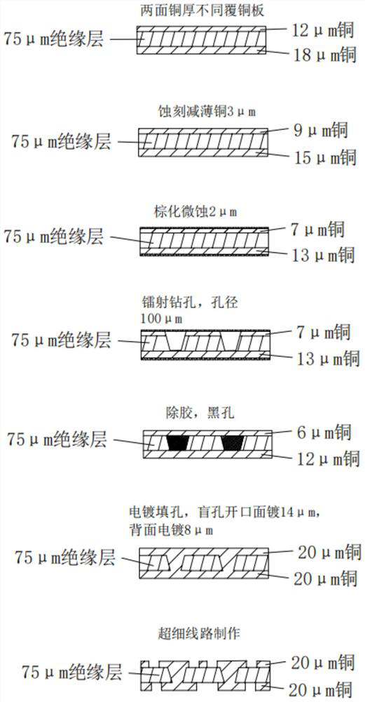
[0039] refer to figure 1 , a method for processing a core layer of a high-density circuit board with arbitrary layers interconnected, comprising the following steps,

[0040] Step 1. Material selection: a double-sided copper-clad laminate, including a dielectric layer with a thickness of 75 μm, an upper copper foil arranged on the top surface of the dielectric layer, and a lower copper foil arranged on the bottom surface of the dielectric layer. The thickness of the upper copper foil is 12μm, the thickness of the lower copper foil is 18μm;

[0041] Step 2. Copper reduction: use a horizontal copper reduction wire to etch the double-sided copper clad laminate in step 1 to reduce the thickness of 3 μm copper. The composition is: concentrated sulfuric acid 4%, hydrogen peroxide 2%, CRICUETCH100 3%, the rest is deionized water, the operating temperature is 30°C, the thickness of the upper copper foil becomes 9 μm after copper reduction, and the thickness of the lower copper foil b...

Embodiment 2

[0053] refer to figure 1 , a method for processing a core layer of a high-density circuit board with arbitrary layers interconnected, comprising the following steps,

[0054] Step 1. Material selection: a double-sided copper-clad laminate, including a dielectric layer with a thickness of 75 μm, an upper copper foil arranged on the top surface of the dielectric layer, and a lower copper foil arranged on the bottom surface of the dielectric layer. The thickness of the upper copper foil is 12μm, the thickness of the lower copper foil is 18μm;

[0055] Step 2. Copper reduction: use a horizontal copper reduction wire to etch the double-sided copper clad laminate in step 1 to reduce the thickness of 3 μm copper. The composition is: 5% concentrated sulfuric acid, 3% hydrogen peroxide, 3% CRICUETCH100, and the rest is deionized water. The operating temperature is 35°C. After copper reduction, the thickness of the upper copper foil becomes 9 μm, and the thickness of the lower copper f...

Embodiment 3

[0067] refer to figure 1 , a method for processing a core layer of a high-density circuit board with arbitrary layers interconnected, comprising the following steps,

[0068] Step 1. Material selection: a double-sided copper-clad laminate, including a dielectric layer with a thickness of 75 μm, an upper copper foil arranged on the top surface of the dielectric layer, and a lower copper foil arranged on the bottom surface of the dielectric layer. The thickness of the upper copper foil is 12μm, the thickness of the lower copper foil is 18μm;

[0069] Step 2. Copper reduction: use a horizontal copper reduction wire to etch the double-sided copper clad laminate in step 1 to reduce the thickness of 3 μm copper. The composition is: 7% concentrated sulfuric acid, 5% hydrogen peroxide, 3% CRICUETCH100, and the rest is deionized water. The operating temperature is 40°C. After copper reduction, the thickness of the upper copper foil becomes 9 μm, and the thickness of the lower copper f...


PUM

PropertyMeasurementUnit
Thicknessaaaaaaaaaa
Thicknessaaaaaaaaaa
Thicknessaaaaaaaaaa

Abstract

The invention discloses a method for processing a core layer of an arbitrary-layer interconnected high-density circuit board, relates to the technical field of circuit boards, and aims to solve the problems that when a blind hole is processed in a copper-clad plate with 12-micron copper foil on both sides, the copper foil at the bottom is thin and can be penetrated by liquid medicine; and after blind hole filling electroplating is completed, surface copper is too thick, and copper needs to be etched and thinned to manufacture a thin circuit. The method is characterized in that: the copper-clad plate with copper foil having different thicknesses (the thickness of the upper copper foil is 12 microns, and the thickness of the lower copper foil is 18 microns) on two sides are customized, after copper reduction and browning, the thicknesses of surface copper are 7 microns and 13 microns respectively, and carbon dioxide laser drilling is performed on the 7-micron copper foil surface; and the copper-clad plate with the copper thickness of 20 microns on both sides is prepared through degumming, hole blackening, hole filling and electroplating, and can be directly used for manufacturing an inner-layer circuit.

Description

technical field [0001] The invention relates to the technical field of circuit boards, in particular to a processing method for a core layer of a high-density circuit board with arbitrary layers interconnected. Background technique [0002] With the increasing demand in the world's electronic consumer goods market, the development of electronic technology has been driven. The functions of electronic products are becoming more and more complex, the performance is getting better and better, and their volume is getting smaller and lighter. Therefore, the requirements for circuit boards are getting higher and higher, which is prominently reflected in the wide application of HDI (HDI: High Density Interconnection) boards. HDI circuit boards are widely used in navigation, medical treatment, transportation, remote communication and other fields. [0003] Car phones, wireless communications, and base stations are all developing in the direction of high-density interconnection, requi...

Claims


Application Information

Patent Timeline
IPC IPC(8): H05K3/42
CPCH05K3/423H05K3/421H05K3/429
Inventor 张渊曾琳张静
Owner 麦德美科技(苏州)有限公司
Why Eureka
Try Eureka