Processing method for printed-circuit connector of PCB of high-speed photoelectric coupling module

A photoelectric coupling and printed plug technology, which is applied in printed circuit manufacturing, electrical components, printed circuits, etc., to improve quality, reduce costs, meet the effects of mass production and safe production

Pending Publication Date: 2021-05-04
HUIZHOU KING BROTHER CIRCUIT TECH +2
View PDF5 Cites 2 Cited by
  • Summary
  • Abstract
  • Description
  • Claims
  • Application Information

AI Technical Summary

Problems solved by technology

The industry mainly adopts the process of front-drawing lead wires, and some patents use the process of inner-layer lead wires (immersion gold + gold fingers), and then cut off the connecting wires through the second drilling proc...

Method used


Image

  • Processing method for printed-circuit connector of PCB of high-speed photoelectric coupling module
  • Processing method for printed-circuit connector of PCB of high-speed photoelectric coupling module

Examples


Embodiment 1

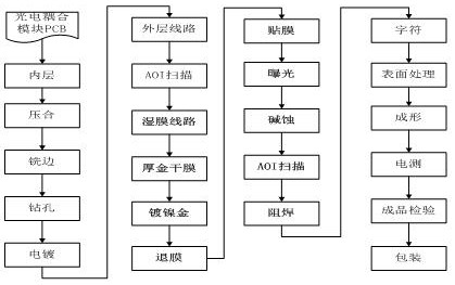
[0040] A processing method for printing a plug PCB with a high-speed photoelectric coupling module, which is characterized in that it includes the following steps: photoelectric coupling module PCB→inner layer→pressing→edge milling→drilling→electroplating→outer layer circuit→AOI scanning→wet film Circuit → thick gold dry film → nickel-plated gold → film removal → lamination → exposure → alkaline etching → AOI scanning → solder mask → characters → surface treatment → forming → electrical measurement → finished product inspection.

[0041] Furthermore, in the outer circuit, each gold finger makes an inner pull lead with a width of 5mil. The junction area of ​​the gold finger lead line set needs to be crossed to the edge of the board in the X and Y directions. The circuit is made according to this file.

[0042] Further, in the AOI scan after the outer circuit, AOI calls the outer engineering data scan with lead wires to confirm the defects, and the CCD magnification of the re-ins...

Embodiment 2

[0056] A processing method for printing a plug PCB with a high-speed photoelectric coupling module, which is characterized in that it includes the following steps: photoelectric coupling module PCB→inner layer→pressing→edge milling→drilling→electroplating→outer layer circuit→AOI scanning→wet film Circuit → thick gold dry film → nickel-plated gold → film removal → lamination → exposure → alkaline etching → AOI scanning → solder mask → characters → surface treatment → forming → electrical measurement → finished product inspection.

[0057] Furthermore, in the outer circuit, each gold finger makes an inner pull lead with a width of 5mil. The junction area of ​​the gold finger lead line set needs to be crossed to the edge of the board in the X and Y directions. The circuit is made according to this file.

[0058] Further, in the AOI scan after the outer circuit, AOI calls the outer engineering data scan with leads to confirm the defect, and the CCD magnification of the re-inspectio...

Embodiment 3

[0072] A processing method for printing a plug PCB with a high-speed photoelectric coupling module, which is characterized in that it includes the following steps: photoelectric coupling module PCB→inner layer→pressing→edge milling→drilling→electroplating→outer layer circuit→AOI scanning→wet film Circuit → thick gold dry film → nickel-plated gold → film removal → lamination → exposure → alkaline etching → AOI scanning → solder mask → characters → surface treatment → forming → electrical measurement → finished product inspection.

[0073] Furthermore, in the outer circuit, each gold finger makes an inner pull lead with a width of 5mil. The junction area of ​​the gold finger lead line set needs to be crossed to the edge of the board in the X and Y directions. The circuit is made according to this file.

[0074] Furthermore, in the AOI scan after the outer circuit, AOI calls the outer engineering data scan with leads to confirm the defect, and the CCD magnification of the re-inspe...


PUM


Abstract

The invention belongs to the technical field of manufacturing of printed circuit boards, and provides a processing method for a printed-circuit connector of a PCB of a high-speed photoelectric coupling module. The processing methodcomprises the following steps: preparation of the PCB of the photoelectric coupling module, preparation of an inner layer, lamination, edge milling, drilling, electroplating, preparation of an outer-layer circuit, AOI scanning, preparation of a wet film circuit, preparation of a thick gold dry film, nickel and gold plating, film stripping, film pasting, exposure, alkaline etching, AOI scanning, resistance welding, character preparation, surface treatment, forming, electric testing and finished product inspection. According to the processing method, a lead is etched after the lead is internally drawn and electroplated with nickel and gold, so the process technology of coating the four sides of the golden finger part of the PCB of the photoelectric coupling module with nickel and gold is realized, the requirements of products on MFG mixed gas testing and salt spray testing are met, and product quality is improved.

Description

technical field [0001] The invention belongs to the technical field of manufacturing printed circuit boards of high-speed photoelectric coupling modules, and in particular relates to a processing method for printing plug PCBs of high-speed photoelectric coupling modules. Background technique [0002] The optoelectronic coupling module is composed of optoelectronic devices, functional circuits and optical interfaces. The optoelectronic devices include two parts: transmitting and receiving. The optical module is mainly responsible for photoelectric conversion. The transmitting end converts the electrical signal into an optical signal. After transmission through the optical fiber, the receiving end converts the optical signal into an electrical signal. [0003] In the photoelectric module market, the rate below 10Gbps basically adopts gold plating + gold finger technology. This process first electroplates the gold finger and then etch the lead wire before etching. Only the u...

Claims


Application Information

Patent Timeline
IPC IPC(8): H05K3/40
CPCH05K3/403H05K3/4007H05K2203/14
Inventor 聂兴培武守坤乔元陈春李享李波樊廷慧
Owner HUIZHOU KING BROTHER CIRCUIT TECH
Why Eureka
Try Eureka