

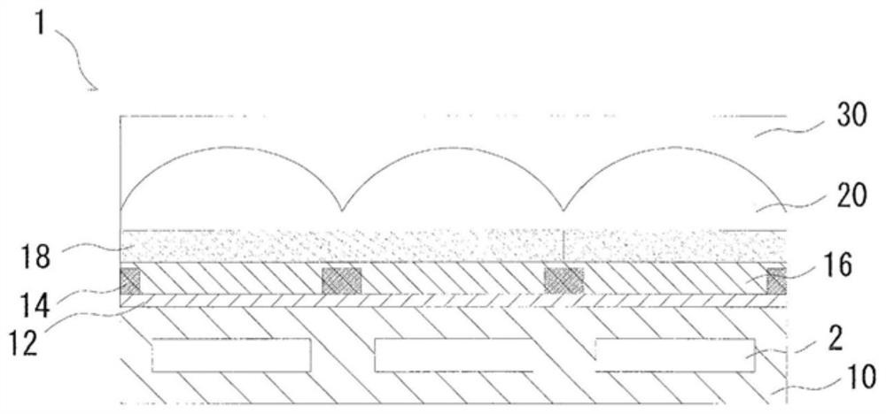
Solid state image sensor
A technology of solid-state imaging elements and structural units, applied in optical elements, photography, instruments, etc., can solve the problem of reducing the amount of light received by the photoelectric conversion part, and achieve the effect of excellent heat resistance and transparency
- Summary
- Abstract
- Description
- Claims
- Application Information
AI Technical Summary
Problems solved by technology
Method used
Image

Examples
preparation example Construction
[0121]
[0122] The composition of the present invention is prepared by, for example, mixing resin (A), component (B) and optionally additives (X) in a predetermined ratio and dissolving them in an organic solvent (G). The prepared radiation-sensitive composition is preferably filtered, for example, with a filter having a pore diameter of about 0.2 μm.
[0123] [Manufacturing method of solid-state imaging device]
[0124] An example of the manufacturing method of the solid-state imaging device of the present invention is described below.
[0125] The method for manufacturing a solid-state imaging device of the present invention includes: a step of forming a coating film of the radiation-sensitive composition of the present invention on at least a microlens; a step of irradiating a part of the coating film with radiation; developing the coating film, removing the coating film formed at other than desired locations; and forming the cured film on the microlens by heating the d...
Embodiment
[0141] Hereinafter, although this invention is demonstrated concretely based on an Example, this invention is not limited to these Examples. "Parts" mean "parts by mass" unless otherwise mentioned.
[0142] [Weight average molecular weight (Mw) and number average molecular weight (Mn)]
[0143] Mw and Mn of the resin were measured by the gel permeation chromatography (GPC) method under the following conditions. In addition, the molecular weight distribution (Mw / Mn) was calculated from the obtained Mw and Mn.
[0144] Device: GPC-101 (manufactured by Showa Denko)
[0145] GPC column: Connect GPC-KF-801, GPC-KF-802, GPC-KF-803, and GPC-KF-804 manufactured by Shimadzu GLC
[0146] Mobile Phase: Tetrahydrofuran
[0147] Column temperature: 40°C
[0148] Flow rate: 1.0mL / min
[0149] Sample concentration: 1.0% by mass
[0150] Sample injection volume: 100uL
[0151] Detector: Differential refractometer
[0152] Standard material: monodisperse polystyrene
[0153] [Synthes...
Synthetic example 1
[0177] [Synthesis Example 1] (Synthesis of Resin (M-1))
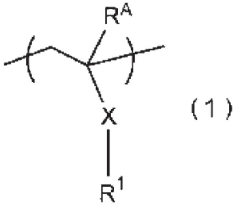
[0178] Into a flask equipped with a cooling tube and a stirrer, 8 parts of 2,2'-azobis(2,4-dimethylvaleronitrile) and 200 parts of diethylene glycol methyl ether were charged. Then, 30 parts of 1,1,1,3,3,3-hexafluoro-2-(4-vinylphenyl)-propan-2-ol, 5 parts of α-methyl-p-hydroxybenzene Ethylene, 20 parts of methacrylic acid-3,4-epoxycyclohexyl methyl ester and 45 parts of N-vinylphthalimide were replaced with nitrogen, slowly stirred, and the temperature of the solution The temperature was raised to 70° C., and the temperature was maintained for 5 hours to perform polymerization, whereby a polymer solution containing the resin (M-1) was obtained. The solid content concentration of the polymer solution was 34% by mass, the Mw of the resin (M-1) was 10,000, and the molecular weight distribution (Mw / Mn) was 2.1.
PUM
| Property | Measurement | Unit |
|---|---|---|
| refractive index | aaaaa | aaaaa |
| carbon number | aaaaa | aaaaa |
| molecular weight distribution | aaaaa | aaaaa |
Abstract
Description
Claims
Application Information