Silicon carbide MOSFET device and cellular structure thereof
A silicon carbide and device technology, applied in semiconductor devices, electric solid state devices, semiconductor/solid state device components, etc., can solve the problems of increased stray inductance, decreased electrical performance of modules, and increased cost of module packaging, so as to reduce parasitic inductance. Capacitance, reduce leakage current, improve the effect of bipolar injection effect
- Summary
- Abstract
- Description
- Claims
- Application Information
AI Technical Summary
Problems solved by technology
Method used
Image

Examples
no. 1 example
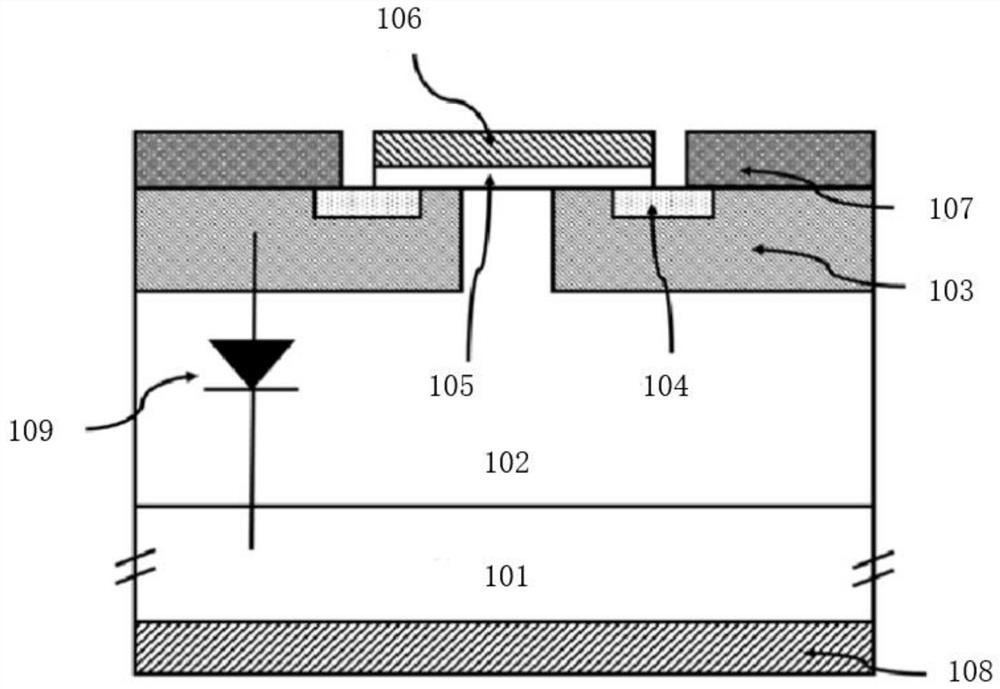
[0067] figure 2 It is a schematic diagram of the cell structure of a split-gate Schottky diode (SBD, hereinafter referred to as SBD) embedded silicon carbide MOSFET device. Such as figure 2 As shown, it includes: first conductivity type substrate 2, first conductivity type drift region 3, Schottky metal 4, polysilicon gate 5, gate insulating layer 6, second conductivity type well region 7, first conductivity type Source region 8 , second conductivity type enhancement region 9 , source metal 10 , and drain metal 11 .
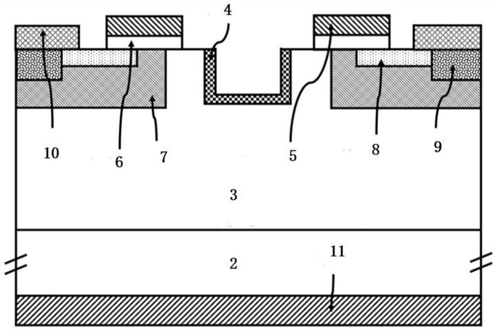
[0068] image 3 It is a schematic diagram of Schottky metal and source metal interconnection and isolation from polysilicon gate. Such as image 3 As shown, it includes: first conductivity type substrate 2, first conductivity type drift region 3, Schottky metal 4, polysilicon gate 5, gate insulating layer 6, second conductivity type well region 7, first conductivity type Source region 8 , second conductivity type enhanced region 9 , source metal 10 , drain...
no. 2 example
[0103] Figure 4 It is a schematic diagram of the inverted trapezoidal groove structure of the cell structure of the silicon carbide MOSFET device. The contents of this embodiment and the first embodiment are basically the same, the difference lies in the following contents:
[0104] The shape of the main groove where the Schottky metal is located is not only a rectangle, but also an isosceles trapezoid, an isosceles triangle, a semicircle, a semiellipse, or other symmetrical geometric shapes.
[0105] In addition, the present invention also sets the second conductivity type shielding layer 14 in the local area where the Schottky metal is in contact with the drift region, which reduces the leakage current when the Schottky junction is reverse biased and improves the electrical performance of the device.
[0106] In the cell structure of the silicon carbide MOSFET device, in this embodiment, a P-type shielding layer is provided in the area where the sidewall of the main trench...
no. 3 example
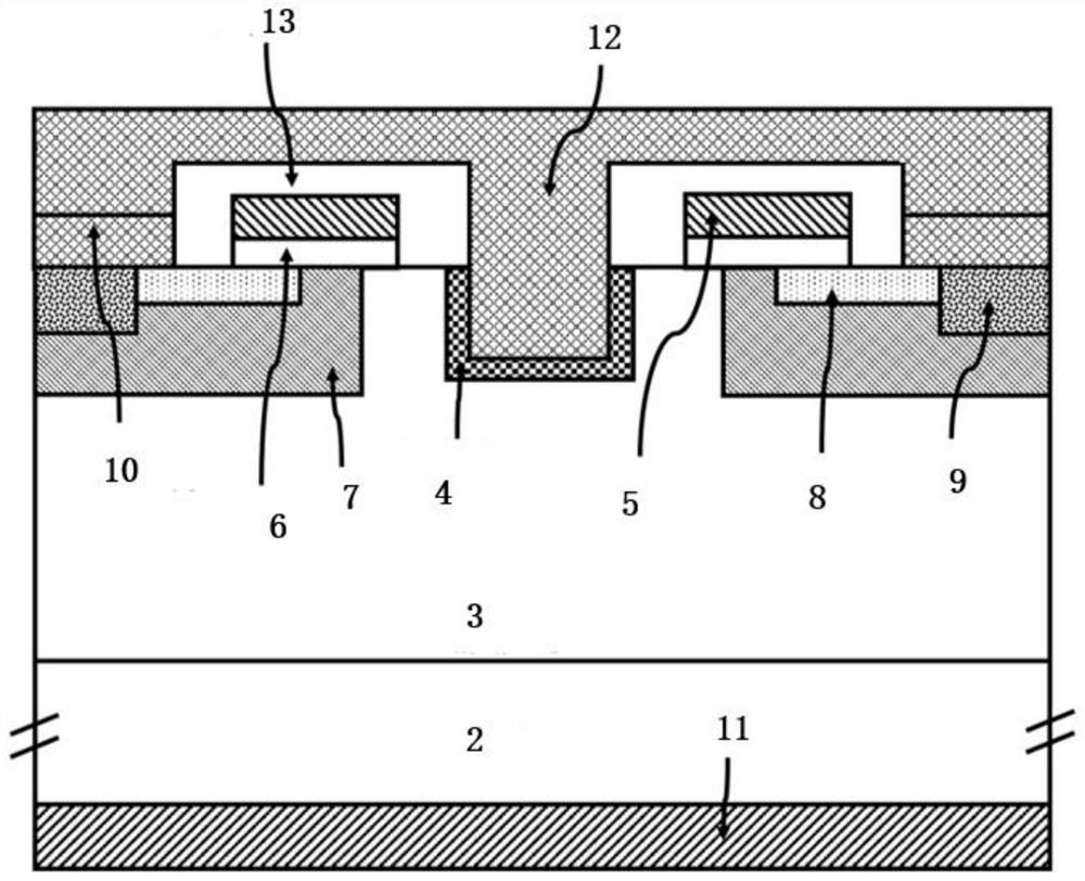
[0109] Figure 5 It is a schematic diagram of a trench silicon carbide MOSFET device with integrated SBD. Such as Figure 5 As shown, it includes: first conductivity type substrate 2, first conductivity type drift region 3, Schottky metal 4, polysilicon gate 5, gate insulating layer 6, second conductivity type well region 7, first conductivity type Source region 8 , second conductivity type enhanced region 9 , source metal 10 , drain metal 11 , source block metal 12 , and interlayer dielectric 13 .
[0110] The first conductivity type substrate 2 in this specification may include various semiconductor elements, such as silicon or silicon germanium of single crystal, polycrystalline or amorphous structure, and may also include mixed semiconductor structures, such as silicon carbide, gallium nitride, Indium phosphide, gallium arsenide, alloy semiconductors or combinations thereof are not limited herein. The first conductivity type substrate 2 in this embodiment is preferably ...
PUM
| Property | Measurement | Unit |
|---|---|---|
| Thickness | aaaaa | aaaaa |
Abstract
Description
Claims
Application Information