Wavelength-locked high-efficiency semiconductor laser and preparation method thereof

A wavelength-locked, semiconductor technology, applied in the field of high-efficiency semiconductor lasers and its preparation, can solve problems such as increased stress, reduced current injection efficiency, and low conductivity

Inactive Publication Date: 2021-05-11
INST OF APPLIED ELECTRONICS CHINA ACAD OF ENG PHYSICS
View PDF8 Cites 2 Cited by
  • Summary
  • Abstract
  • Description
  • Claims
  • Application Information

AI Technical Summary

Problems solved by technology

Due to the relatively high doping of the P-type confinement layer and the contact layer, the conductivity is low, and it is easy to produce lateral expansion under high current density injection, resulting in a decrease in current injection efficiency.
By etching the material on both sides of the ridge, the current spread can be suppressed, but at the same time, problems such as increased lateral divergence angle, increased stress, and polariz

Method used


Image

  • Wavelength-locked high-efficiency semiconductor laser and preparation method thereof
  • Wavelength-locked high-efficiency semiconductor laser and preparation method thereof
  • Wavelength-locked high-efficiency semiconductor laser and preparation method thereof

Examples


Embodiment 1

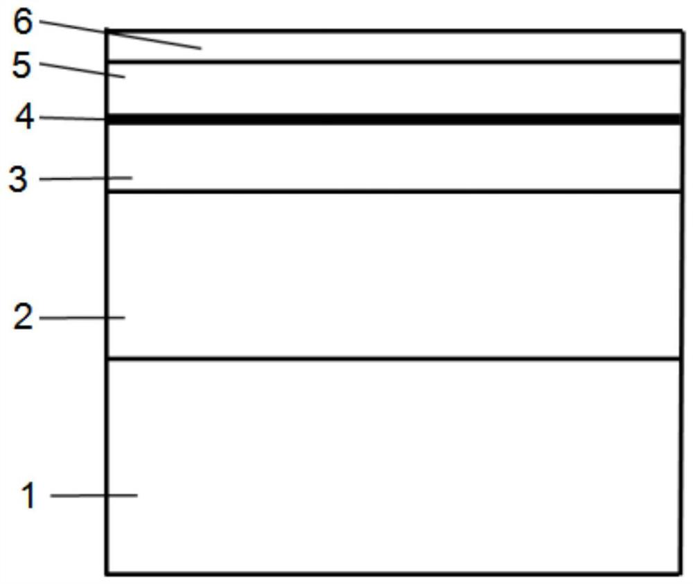
[0044] In this embodiment, a wavelength-locked high-efficiency semiconductor laser is provided, so as to improve chip efficiency and realize on-chip spectral locking through the high-efficiency semiconductor laser. The specific design of the high-efficiency semiconductor laser is as follows:

[0045] Based on the substrate layer, the conductivity type of the substrate layer is N type, and GaAs is used as the substrate.

[0046] The lower confinement layer, the lower waveguide layer, the quantum well active layer, the upper waveguide layer, the insertion layer, the upper confinement layer and the contact layer are arranged in sequence from the substrate layer, wherein the conductivity type of the lower confinement layer is N type, using ( Al 0.4 Ga 0.6 ) 0.51 In 0.49 Made of P material and the growth thickness is 1000nm; the conductivity type of the lower waveguide layer is N type, using Ga 0.51 In 0.49 Made of P material and the growth thickness is 1100nm; the quantum we...

Embodiment 2

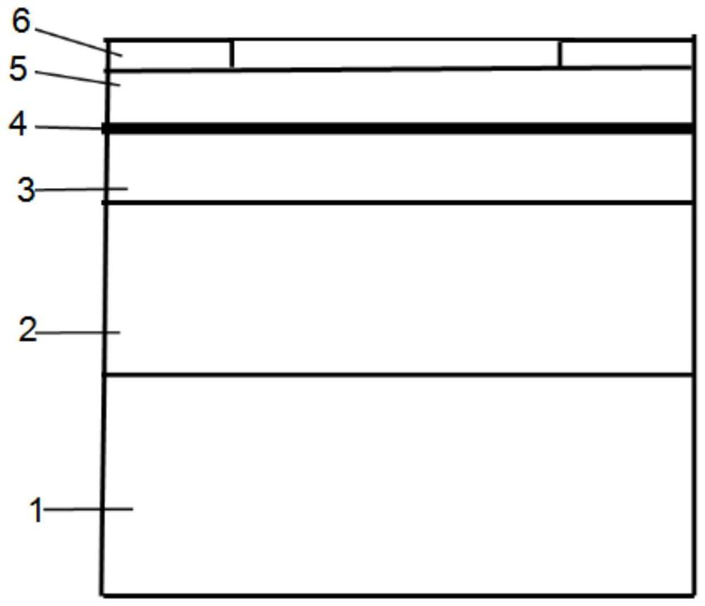
[0051] Embodiment 1 specifically discloses a wavelength-locked high-efficiency semiconductor laser. In order to realize effective processing and manufacturing of the semiconductor laser, a method for preparing a wavelength-locked high-efficiency semiconductor laser is also provided in this embodiment. The preparation method is as follows:

[0052] S1: sequentially grow the lower confinement layer, lower waveguide layer, quantum well active layer, upper waveguide layer and insertion layer on the substrate layer to form the first epitaxial structure; figure 1 As shown, the details are as follows:

[0053] The conductivity type of the lower confinement layer is N-type, using (Al 0.4 Ga 0.6 ) 0.51 In 0.49 Made of P material with a growth thickness of 1000nm;

[0054] The conductivity type of the lower waveguide layer is N-type, using Ga 0.51 In 0.49 Made of P material with a growth thickness of 1100nm;

[0055] Quantum well active layer is GaAs 0.8 P 0.2 material and a t...


PUM

PropertyMeasurementUnit
Thicknessaaaaaaaaaa

Abstract

The invention discloses a wavelength-locked high-efficiency semiconductor laser, and belongs to the technical field of semiconductor laser devices. The laser comprises an N-type lower limiting layer, an N-type lower waveguide layer, a quantum well active layer, a P-type upper waveguide layer, an insertion layer, a P-type upper limiting layer and a P-type contact layer from an N-type substrate layer to the top in sequence, the refractive index of the insertion layer is the same as that of the P-type waveguide layer, the conduction type of the insertion layer is N-type, a current limiting layer is formed in the slow axis direction, meanwhile, a grating is formed in the resonance direction, current injection and the grating are formed by etching the insertion layer, and then the P-type upper limiting layer and the P-type contact layer are grown through a secondary epitaxial process. A high-reflection film is evaporated on the rear cavity surface of the laser, and an anti-reflection film is evaporated on the front cavity surface of the laser. The grating is integrated on a laser sheet, meanwhile, good lateral current limitation is formed, the grating and the current limiting layer adopt the same process, the preparation process is simplified, and the laser has the advantages of wavelength locking and high electro-optical efficiency.

Description

technical field [0001] The invention belongs to the technical field of semiconductor laser devices, and in particular relates to a wavelength-locked high-efficiency semiconductor laser and a preparation method thereof. Background technique [0002] Semiconductor lasers are widely used in pumping solid-state and fiber lasers, material processing, and laser medical treatment due to their advantages such as compact structure, low cost, and easy control of the optical field. At present, many application scenarios require semiconductor lasers to have the characteristics of high efficiency and narrow spectral width. [0003] One of the important factors affecting the efficiency of semiconductor lasers is the lateral current spread. Since the doping of the P-type confinement layer and the contact layer is relatively high and the electrical conductivity is low, it is easy to generate lateral expansion under high current density injection, resulting in a decrease in current injectio...

Claims


Application Information

Patent Timeline
IPC IPC(8): H01S5/20H01S5/042H01S5/12H01S5/343
CPCH01S5/0425H01S5/12H01S5/2009H01S5/343
Inventor 周坤杜维川何林安李弋高松信唐淳
Owner INST OF APPLIED ELECTRONICS CHINA ACAD OF ENG PHYSICS
Why Eureka
Try Eureka