Component prepared from laser processing diamond material and preparation method of component

A technology of laser processing and components, applied in laser welding equipment, metal processing equipment, welding equipment, etc., can solve the problem that the conductivity of the substrate material or the carrier concentration change range is limited, it is difficult to have a high modulation depth of electromagnetic waves, and the modulation is restricted The depth of modulation of the device and other issues can be easily met, and the effects of good thermal conductivity and high precision can be achieved.

Inactive Publication Date: 2021-05-25
TIANJIN UNIV
View PDF7 Cites 4 Cited by
  • Summary
  • Abstract
  • Description
  • Claims
  • Application Information

AI Technical Summary

Problems solved by technology

[0003] Some components such as electromagnetic wave modulators are mainly realized based on the photolithography technology of Si substrate, such as the Chinese invention patent with application number 202010166069.7. This technology is etched on the Si surface, and the structure realizes the modulation of electromagnetic waves. The transmittance of electromagnetic waves is low. In addition, the etching structure is limited by the processing accuracy and the structure itself. It is difficult to achieve a high modulation depth for the electromagnetic waves of the target band.
Another example is the Chinese patent application with application numbers 201911264503.9 and 201810223513.7, which discloses an electromagnetic wave modulator that electrically induces changes in substrate conductivity or carrier concentration. However, the range of change in substrate material conductivity or carrier concentration Limited, unable to achieve complete phase change, thus restricting the modulation depth of the modulator

Method used


Image

  • Component prepared from laser processing diamond material and preparation method of component
  • Component prepared from laser processing diamond material and preparation method of component

Examples


Embodiment Construction

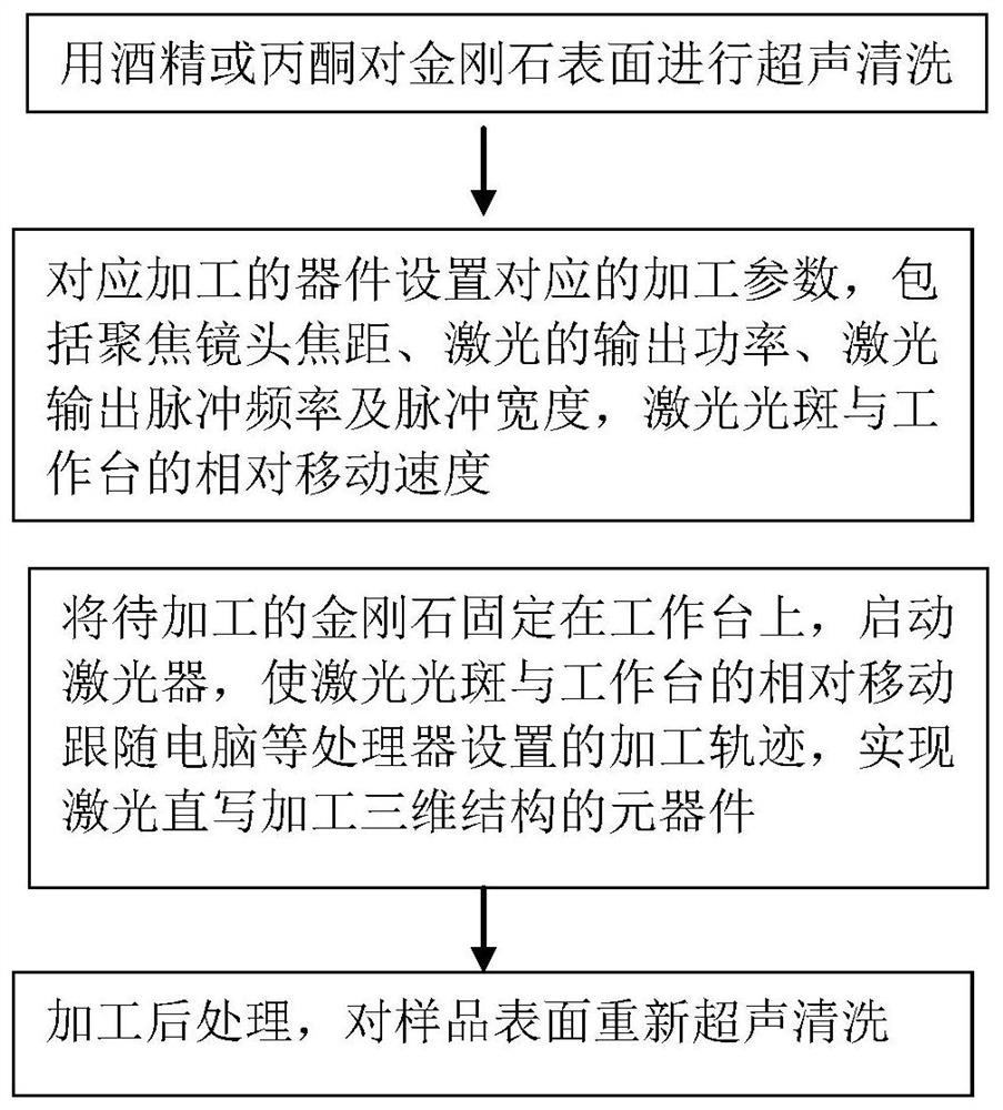
[0021] In order to further understand the invention content, characteristics and effects of the present invention, the following embodiments are enumerated hereby, and detailed descriptions are as follows in conjunction with the accompanying drawings:

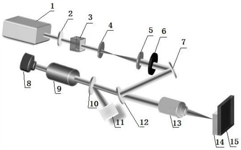
[0022] See Figure 1 to Figure 2 , a kind of method that prepares components and parts with laser processing diamond material, adopt following device: laser device, the beam shutter 6 that is used to control the laser output of laser device, the workbench 15 that places diamond material 14; A focusing lens 13 for focusing is arranged between them; the laser light emitted by the laser passes through the focusing lens 13 and is irradiated on the diamond material 14 on the worktable 15; by controlling the relative movement of the laser spot and the worktable 15, the laser is focused on the diamond surface or inside; by adjusting the optical characteristic parameters of the focusing lens, the output power of the laser, the pulse re...


PUM

PropertyMeasurementUnit
frequencyaaaaaaaaaa
Vickers hardnessaaaaaaaaaa
frequencyaaaaaaaaaa

Abstract

The invention discloses a method for preparing a component by processing a diamond material through laser. The method adopts following devices: a laser device, a light beam shutter for controlling the output of the laser device, and a workbench for placing a diamond, a focusing lens is arranged between a laser head of the laser device and the workbench; laser emitted by the laser device is irradiated on the diamond through the focusing lens; the laser is focused on the surface or inside the diamond by controlling the relative movement of a laser spot and the workbench; and the diamond material in a laser radiation area is converted into a graphite phase and an amorphous carbon phase by adjusting the output power of the laser device, the pulse repetition frequency of laser output and the three-dimensional moving speed of the laser spot relative to the workbench, and the conductivity and the electromagnetic wave transmittance of the material in the laser radiation area are changed. The invention further discloses a component prepared by the method. Various devices such as an electromagnetic wave modulator, a resistor and a capacitor which are freely designed can be processed on the surface and the interior of the diamond.

Description

technical field [0001] The invention relates to an electromagnetic wave modulation device and a preparation method thereof, in particular to a component prepared by laser processing diamond material and a preparation method thereof. Background technique [0002] At present, laser technology continues to develop, and its application has penetrated into the fields of material science, optoelectronic devices, 3D printing, and biomedicine. Compared with the long-pulse laser, the pulse width of the ultrashort-pulse laser is extremely short. When the laser is applied to the target material, no significant damage will occur near the focus area, and the effects of heat conduction in a short period of time can be ignored. With the development of science and technology, microelectronics technology has significantly promoted the development of the information society. At present, silicon materials still occupy more than 90% of the field of semiconductor materials, and the new generatio...

Claims


Application Information

Patent Timeline
Patent Type & Authority Applications(China)
IPC IPC(8): B23K26/04B23K26/064B23K26/362B23K26/53B23K26/70
CPCB23K26/064B23K26/04B23K26/702B23K26/362B23K26/53
Inventor 庞冬青林百川宋琦柴路胡明列
Owner TIANJIN UNIV
Why Eureka
Try Eureka