A kind of preparation method of ceramic copper clad laminate

A technology of ceramic copper clad laminate and ceramic substrate, used in chemical instruments and methods, metal layered products, layered products, etc., can solve the problem of unreliable connection between ceramics and copper foil, holes in the welding layer, low thermal cycle life, etc. problem, to achieve the effect of reducing porosity, reducing sintering temperature, and improving strength

Active Publication Date: 2022-07-26
CHINALCO MATERIALS APPL RES INST CO LTD
View PDF0 Cites 0 Cited by
  • Summary
  • Abstract
  • Description
  • Claims
  • Application Information

AI Technical Summary

Problems solved by technology

[0005] Aiming at the current domestic problems such as holes in the welding layer after the connection between ceramics and copper foil, warpage after welding, and low thermal cycle life, the present invention proposes a preparation method for highly reliable ceramic copper-clad laminates and its supporting active solder. The present invention adopts low melting point , high alloying, no residual active metal solder paste after welding to prepare ceramic copper clad laminates with low post-soldering holes, controllable warpage, and high thermal cycle life, which solves the current problem of unreliable connection between ceramics and copper foil, and helps ceramics Wide application of copper clad laminates in new energy vehicles and high-speed rail locomotives

Method used


Image

  • A kind of preparation method of ceramic copper clad laminate

Examples


preparation example Construction

[0022] A preparation method of a ceramic copper clad laminate of the present invention comprises the following steps:

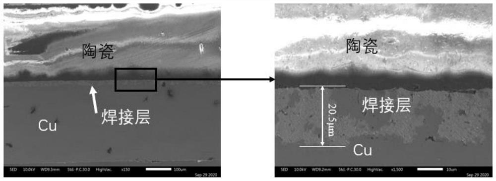
[0023] (1) Active metal solder composition design, vacuum high-pressure gas atomization, powder sieving: After powdering the active metal solder, sieve the powder to obtain an active metal solder powder with a particle size of 5 μm-20 μm; the components of the active metal solder Its mass percentage is: Cu21%-24%, Sn 5%-10%, In 5%-10%, Ti 3%-5%, the balance is Ag, and the proportion of alloy; wherein, the purity of Cu is greater than 99.99wt%, the purity of Sn is greater than 99.99wt%, the purity of In is greater than 99.99wt%, the purity of Ti is greater than 99.99wt%, and the purity of Ag is greater than 99.99wt%. The active metal solder is pulverized by vacuum high-pressure gas atomization. The process conditions of vacuum high-pressure gas atomization are: the vacuum degree of the pulverizing equipment is raised to higher than 1×10 -1 Pa, then heat the a...

Embodiment 1

[0030]The active metal solder is vacuum cast, and the components and mass percentages of the active metal solder are: Cu22.5%, In10%, Sn 5%, Ti 4.5%, and the balance is Ag. The purity of each metal is higher than 99.99wt%; raise the vacuum degree of the milling equipment to higher than 1×10 -2 Pa, then the active metal solder was heated to 1000°C, and after reaching the temperature, the temperature was maintained for 20min.

[0031] Then carry out vacuum high pressure gas atomization powder, the atomization temperature is 1100 ℃, and the atomization gas flow rate is 35m 3 / min, the melt flow rate of the active metal solder is 9.0 kg / min, and the atomizing gas pressure is 0.8 MPa to obtain alloy powder. Using an ultrasonic vibration sieve powder machine, sieve out the active metal solder powder with a particle size of 5μm-20μm.

[0032] According to the weight percentage, take 42% terpineol, 28% diethylene glycol monobutyl ether, 10% polyethanol 2000, 10% modified hydrogenate...

Embodiment 2

[0038] The active metal solder is vacuum casted. The components and mass percentage of the active metal solder are: Cu21.5%, In10%, Sn 10%, Ti 4%, and the balance is Ag. The purity of each metal is higher than 99.99wt%; raise the vacuum degree of the milling equipment to higher than 1×10 -2 Pa, then the active metal solder was heated to 1000°C, and after reaching the temperature, the temperature was maintained for 20min.

[0039] Then carry out vacuum high pressure gas atomization powder, the atomization temperature is 1100 ℃, and the atomization gas flow rate is 35m 3 / min, the melt flow rate of the active metal solder is 9.0 kg / min, and the atomizing gas pressure is 0.8 MPa to obtain alloy powder. Using an ultrasonic vibration sieve powder machine, sieve out the active metal solder powder with a particle size of 5μm-20μm.

[0040] According to the weight percentage, take 42% terpineol, 28% diethylene glycol monobutyl ether, 10% polyethanol 2000, 10% modified hydrogenated c...


PUM

PropertyMeasurementUnit
particle diameteraaaaaaaaaa
thicknessaaaaaaaaaa
thicknessaaaaaaaaaa

Abstract

The invention discloses a preparation method of a ceramic copper clad laminate, comprising the following steps: (1) powdering active metal solder and then sieving the powder to obtain active metal solder powder with a particle size of 5 μm-20 μm; components of the active metal solder and its mass percentage content is: Cu 21%-24%, Sn 5%-10%, In 5%-10%, Ti 3%-5%, and the balance is Ag; (2) the mass ratio is (85 -90): (10-15) active metal solder powder is mixed with active solder carrier to prepare active solder paste; (3) active solder paste layer is printed on the surface of the ceramic substrate; (4) active solder paste is printed on the surface; The ceramic substrate of the paste layer is placed in a vacuum furnace for debinding; (5) vacuum sintering is performed after assembling the debinding ceramic substrate and copper foil to obtain a ceramic copper clad laminate. The ceramic copper-clad laminate prepared by the invention has low voids after welding, controllable warpage and high thermal cycle life.

Description

technical field [0001] The invention belongs to the technical field of electronic packaging, and particularly relates to a preparation method of a ceramic copper clad laminate. Background technique [0002] Insulate-Gate Bipolar Transistor (IGBT) is a bipolar device with MOS structure, which has the advantages of bipolar transistor and field effect transistor, and has fast switching speed, high operating frequency, low driving power and safe working area. It is the most important high-power device in the field of power electronics. It is widely used in electric vehicles, high-speed rail locomotives, smart grids and other fields, and is the core "core" of the green economy. [0003] Ceramic CCL is a composite material of copper-ceramic-copper three-layer structure. It has the characteristics of high heat dissipation, high insulation, high mechanical strength, thermal expansion and chip matching of ceramics, and also has the characteristics of strong current carrying capacity...

Claims


Application Information

Patent Timeline
Patent Type & Authority Patents(China)
IPC IPC(8): B32B15/04C04B41/88
CPCC04B41/88C04B41/5161C04B41/515C04B41/5133C04B41/5127C04B41/5116C04B41/4539C04B41/0072
Inventor 蔡正旭娄花芬王云鹏莫永达
Owner CHINALCO MATERIALS APPL RES INST CO LTD
Why Eureka
Try Eureka