Anti-PID-effect double-sided battery and preparation method thereof

A double-sided battery, effect technology, applied in the direction of circuits, photovoltaic power generation, electrical components, etc.

Pending Publication Date: 2021-05-28
TONGWEI SOLAR ENERGY CHENGDU CO LID
View PDF11 Cites 0 Cited by
  • Summary
  • Abstract
  • Description
  • Claims
  • Application Information

AI Technical Summary

Problems solved by technology

[0010] The purpose of the present invention is to overcome the disadvantages that it is difficult to effectively improve the PID attenuation phenomenon on the back of the double-sided battery by using existing methods, and to provide a double-sided battery with anti-PID effect and its preparation method

Method used


Image

  • Anti-PID-effect double-sided battery and preparation method thereof

Examples


Embodiment 1

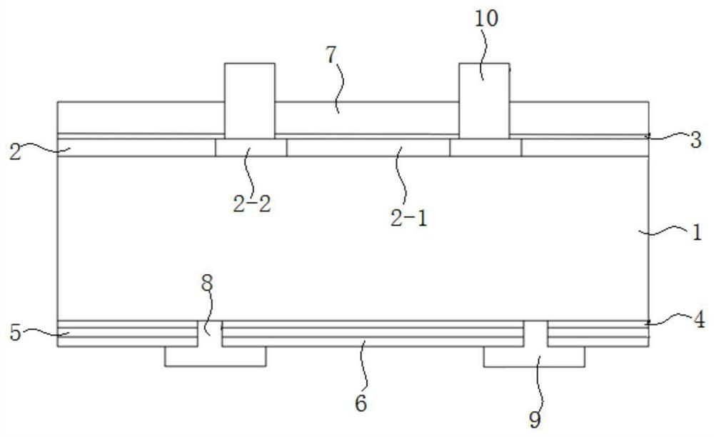
[0048] like figure 1 As shown, the back cell of this embodiment includes a silicon wafer base 1, and the front side of the silicon wafer base 1 is provided with a front emitter 2, a front oxide layer 3, a front silicon nitride passivation and an anti-reflection layer 7 sequentially from bottom to top. And a positive electrode 10, the back of which is provided with an aluminum oxide passivation layer 4, a silicon oxide film 5, a silicon nitride passivation and protection layer 6, and a rear sub-gate electrode 9 in sequence from top to bottom.

[0049] The preparation method of the rear battery of this embodiment specifically includes the following process steps:

[0050] 1. Texture making: use single crystal P-type silicon wafer substrate 1, and use alkali to make texturing on the front and back to form a textured structure.

[0051] 2. Diffusion: React the silicon wafer after texturing with phosphorus oxychloride and the silicon wafer at high temperature to make the front dif...

Embodiment 2

[0070] The structure of the back battery of this embodiment is the same as that of Example 1, and the preparation method of the back battery of this embodiment specifically includes the following process steps:

[0071] 1. Texture making: Single crystal P-type silicon wafers are used, and alkali is used to make texturing on the front and back to form a textured structure.

[0072] 2. Diffusion: React the silicon wafer after texturing with phosphorus oxychloride and the silicon wafer at high temperature to make the front diffuse to form a PN emitter junction 2. Diffusion is carried out by the above-mentioned diffusion process, and the square resistance of the thin layer on the front surface after diffusion is between 150Ω / □.

[0073] 3. Laser SE: use the diffused phosphosilicate glass as the phosphorus source, and perform laser doping on the front side of the diffused silicon wafer and the metallized area corresponding to the positive electrode grid line to form a heavily doped...

Embodiment 3

[0091] The structure of the back battery of this embodiment is the same as that of Example 1, and the preparation method of the back battery of this embodiment specifically includes the following process steps:

[0092] 1. Texture making: use single crystal P-type silicon wafer substrate 1, and use alkali to make texturing on the front and back to form a textured structure.

[0093] 2. Diffusion: React the silicon wafer after texturing with phosphorus oxychloride and the silicon wafer at high temperature to make the front diffuse to form a PN emitter junction (that is, the front emitter 2). Diffusion is carried out by the above-mentioned diffusion process, and the sheet resistance of the thin layer on the front surface after diffusion is between 120 Ω / □.

[0094] 3. Laser SE: use the diffused phosphosilicate glass as the phosphorus source, and perform laser doping on the front side of the diffused silicon wafer and the metallized area corresponding to the positive electrode gr...


PUM

PropertyMeasurementUnit
Sheet resistanceaaaaaaaaaa
Total thicknessaaaaaaaaaa

Abstract

The invention discloses an anti-PID-effect double-sided battery and a preparation method thereof, and belongs to the technical field of battery preparation. According to the preparation method of the anti-PID-effect double-sided battery, a layer of silicon oxide film is grown between a back aluminum oxide passivation layer and a back silicon nitride passivation and the protection layer of thedouble-sided battery by adopting an atomic layer deposition or plasma enhanced atomic layer deposition mode, so that on the basis that the passivation effect of an aluminum oxide field is not influenced, alkali metal ions are effectively prevented from entering the surface of the silicon wafer, and polarization and corrosive PID failure caused by the alkali metal ions is reduced. Meanwhile, on the interface of the aluminum oxide and the silicon nitride, the polarization effect caused by the K+center in the silicon nitride can be effectively reduced, and the PID failure caused by the silicon nitride layer is reduced.

Description

technical field [0001] The invention belongs to the technical field of battery preparation, and more specifically relates to a double-sided battery with anti-PID effect and a preparation method thereof. Background technique [0002] Potential induced degradation (PID) refers to the phenomenon of power attenuation of solar cell modules under a certain external voltage for a long time. This phenomenon was first discovered by Sunpower in 2005. According to the statistics of relevant authoritative organizations, the attenuation of power generation of photovoltaic power plants caused by PID can reach more than 30%, which has become one of the most important reasons for the attenuation of output efficiency of photovoltaic power plants and has become a major problem in the application of modules. [0003] Regarding the PID failure mechanism, it has been extensively studied by the industry and recognized as follows: In grid power generation, many photovoltaic modules are connected ...

Claims


Application Information

Patent Timeline
IPC IPC(8): H01L31/18H01L31/0216H01L31/068C23C16/40C23C16/455C23C16/50
CPCH01L31/1804H01L31/1868H01L31/02167H01L31/02168H01L31/0684C23C16/402C23C16/45525C23C16/45536Y02E10/547Y02P70/50
Inventor 黄智张林张鹏刘秋阳李红飞李宁郑傲然徐冠群徐涛翟绪锦谢泰宏
Owner TONGWEI SOLAR ENERGY CHENGDU CO LID
Why Eureka
Try Eureka