Electron source package

An electron source and power supply technology, applied in the manufacture of circuits, electrical components, electrode systems, etc., can solve the problems of large transport resistance, large degree of surface damage, and reduced collection efficiency of nanowire array photocathode, so as to improve the absorption rate , reduce the probability of emission, and enhance the effect of quantum efficiency

Active Publication Date: 2021-06-04
NANJING UNIV OF SCI & TECH
View PDF2 Cites 0 Cited by
  • Summary
  • Abstract
  • Description
  • Claims
  • Application Information

AI Technical Summary

Problems solved by technology

[0003] Although the quantum efficiency is improved by using the nanowire array structure, in order to better meet the emission requirements of the electron source, the concentration of the electron beam emitted by the cathode of the AlGaN nanowire array can be further improved
At present, AlGaN nanowires use a single Al component. The incident light is irradiated on the nanowire array to generate electrons, and the single Al component has a large resistance to the transport of electrons in the photoemissive material. Therefore, the single-component AlGaN nanowires Arrays do not further improve photoemission performance of photocathode
In addition, the single Al component nanowire array has a disadvantage, that is, when a single nanowire forms an array, the electrons escaping from the side of the nanowire will be absorbed twice by the adjacent nanowires, resulting in an electron shielding effect.
The electrons escaped from the side can only be collected by the collection side on the top surface if they exit within the corresponding angle, otherwise they will be captured by the adjacent nanowires and cannot escape the array structure, thus reducing the photocathode density of the nanowire array. The collection efficiency of the electron beam may even cause divergence, so that the nanowire array photocathode cannot meet the requirements of the electron source for the concentration of the electron beam.
[0004] Now for heterojunction Al x Ga 1-x The proposed growth method of the N / GaN nanowire array structure mainly adopts the etching method, but etching will destroy the Al component content on the sidewall of the nanowire array, and the heterojunction Al obtained by etching x Ga 1- x The diameter of the N / GaN nanowire array is relatively large, and the degree of surface damage is relatively large, so it is urgent to obtain heterojunction Al with high growth quality by improving the growth method. x Ga 1-x Array of N / GaN nanowires

Method used


Image

  • Electron source package
  • Electron source package
  • Electron source package

Examples


Embodiment 1

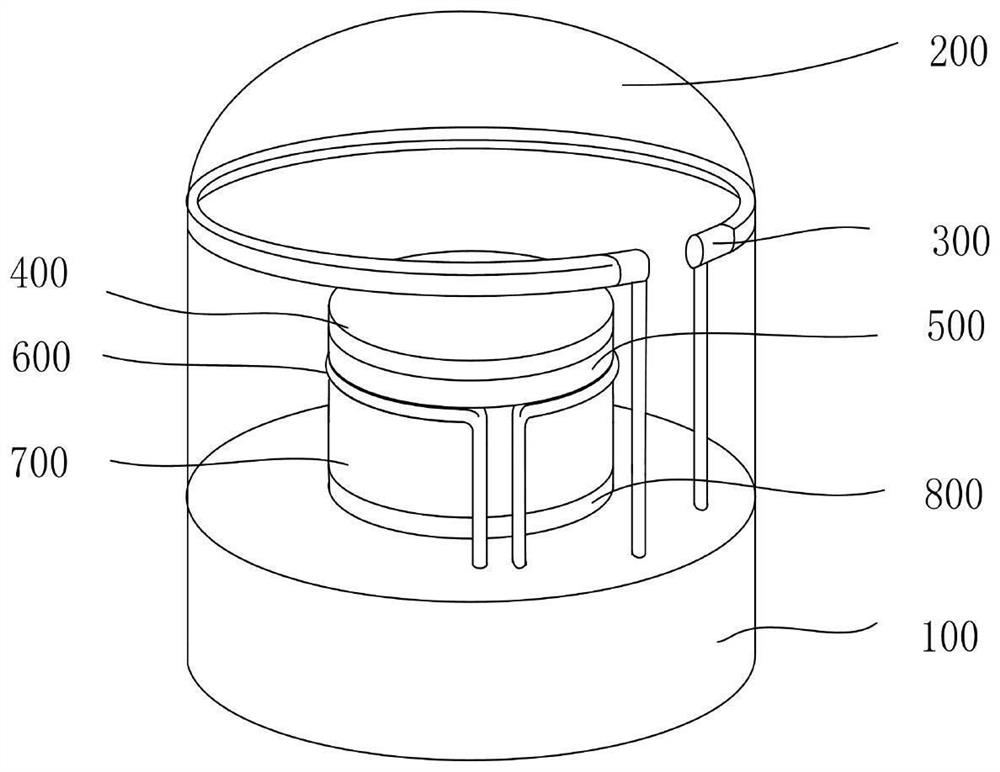
[0018] combine Figure 1-Figure 3 , which is the first embodiment of the present invention, provides an electron source package for photoemission by external photoelectric effect, including a substrate 100, a sealing cover 200, and an electron source. The substrate 100 is used to carry the electron source, the sealing cover 200 cooperates with the substrate 100 to form a closed space, and the electron source emits electrons under the external photoelectric effect. Specifically, the substrate 100 includes a substrate housing and a power circuit disposed in the substrate housing. The substrate housing not only protects the power circuit, but also supports the electron source. The sealing cover 200 is a transparent cover to seal and form a vacuum environment, and the transparent material is convenient for subsequent devices to collect overflowing electrons.

[0019] Further, the power supply circuit includes a bias voltage circuit.

[0020] Further, the electron source includes...

Embodiment 2

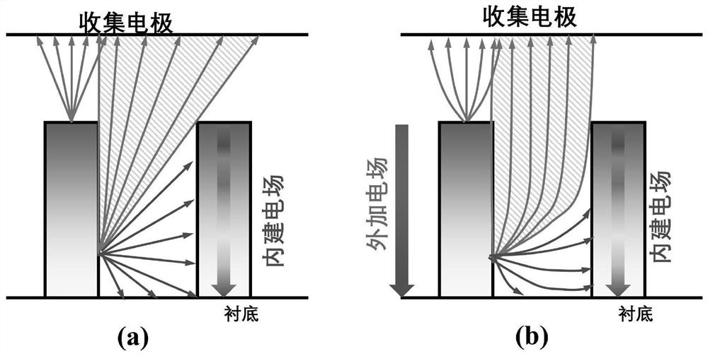
[0025] combine Figure 4 , 5 , is the second embodiment of the present invention. The difference between this embodiment and the first embodiment is that a nanowire structure and growth environment are provided. In this embodiment, the nanowire 700 is grown on the substrate 800 . The surface of the substrate 800 includes several raised structures 820 , and each nanowire 700 in the nanowire bundle grows on the corresponding raised structures 820 . Nanowires can be grown on the raised structure 820, which can make the nanowires grow in an orderly and fixed position, and the grown array has a fixed period and adjustable diameter; at the same time, the method of growing nanowires on the raised structure The formation of dense arrays can be avoided, and the electrons emitted from the side have more possibilities to move to the top collecting electrode, reducing the probability of being repeatedly absorbed by adjacent nanowires.

[0026] Further, each nanowire 700 of the nanowire...

Embodiment 3

[0031] combine Figure 6 , which is the third embodiment of the present invention, provides a method for making the nanowires involved in the second embodiment, including producing neatly arranged nano-scale SiO on the surface of the substrate 2 Masking method, growing heterojunction Al x Ga 1-x Method of N nanowire array and fabrication into heterojunction Al x Ga 1-x The invention discloses a preparation method of an N / GaN nanowire array electron source cathode.

[0032] Step S100, producing neatly arranged nano-scale SiO on the surface of the substrate 2 Mask method:

[0033] Step S101, cleaning the sapphire Al with acetone, alcohol and deionized water with a volume ratio of 1:1:2 2 o 3 substrate, on sapphire Al 2 o 3 On the (0001) surface, a layer of GaN thin film is grown by MOCVD method, and the layer thickness is 1.5mm;

[0034] Step S102, depositing a layer of SiO on the GaN film by radio frequency sputtering 2 , with a thickness of 40nm; through electron be...


PUM

PropertyMeasurementUnit
diameteraaaaaaaaaa
lengthaaaaaaaaaa
lengthaaaaaaaaaa

Abstract

The invention provides an electron source package, which comprises a substrate, a sealing cover and an electron source. A power supply is arranged in the substrate, the sealing cover is arranged on the substrate and forms a closed space with the substrate, and the electron source is arranged on the substrate in the closed space. The electron source comprises a substrate, a nanowire harness, an electrode ring, an anti-reflection layer and a protective layer. The substrate is arranged on the substrate and grounded, the nanowire harness is arranged on the substrate, the electrode ring is arranged above the nanowire harness and electrically connected with a substrate power source, the anti-reflection layer is arranged on the electrode ring, and the protective layer is arranged on the anti-reflection layer.

Description

technical field [0001] The invention relates to a vacuum electron source packaging technology, in particular to an electron source packaging technology. Background technique [0002] With the rise of nanotechnology, nanomaterials are playing an increasingly important role in many fields. The nanowire array structure is a new type of quasi-one-dimensional nanostructure, which has new physical or chemical properties different from thin film materials. The light absorption effect occurs when photons touch the nanoscale array on the surface, and the photons that are not absorbed but pass through will be absorbed due to reflection or refraction, and it is difficult to escape, forming a "photon capture effect", which improves the photon absorption effect. The absorption rate can further improve the quantum efficiency of the photocathode. [0003] Although the quantum efficiency is improved by adopting the nanowire array structure, in order to better meet the emission requirement...

Claims


Application Information

Patent Timeline
Patent Type & Authority Applications(China)
IPC IPC(8): H01J1/308H01J1/34H01J9/26H01J9/12
CPCH01J1/308H01J1/34H01J9/26H01J9/12
Inventor 刘磊陆菲菲田健张杨星月
Owner NANJING UNIV OF SCI & TECH
Why Eureka
Try Eureka