Two-dimensional ferroelectric semiconductor channel ferroelectric dielectric layer field effect transistor and preparation method thereof

A technology of field effect transistors and semiconductors, applied in the field of effect transistors, can solve problems such as incompatibility with silicon-based semiconductor manufacturing processes, difficulty in achieving stable non-volatile storage, and prolonging the remnant polarization of ferroelectrics, achieving good application prospects and improving Device stability, the effect of reducing remanent polarization loss

Active Publication Date: 2021-06-15
UNIV OF ELECTRONICS SCI & TECH OF CHINA
View PDF11 Cites 7 Cited by
  • Summary
  • Abstract
  • Description
  • Claims
  • Application Information

AI Technical Summary

Problems solved by technology

[0005] In view of the above deficiencies, the present invention provides a two-dimensional ferroelectric semiconductor channel ferroelectric dielectric layer field effect transistor and its preparation method. By combining the two ferroelectrics with each other, the bound charges of the two at the interface will meet The charge shielding by the depolarization field can prolong the remnant polarization of the ferroelectric, effectively solving the problems in the prior art that it is difficult to achieve stable non-volatile storage and incompatibility with silicon-based semiconductor manufacturing processes.

Method used


Image

  • Two-dimensional ferroelectric semiconductor channel ferroelectric dielectric layer field effect transistor and preparation method thereof
  • Two-dimensional ferroelectric semiconductor channel ferroelectric dielectric layer field effect transistor and preparation method thereof

Examples


Embodiment 1

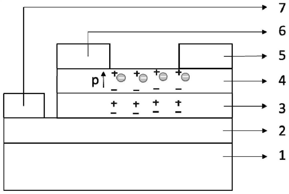
[0028] A two-dimensional ferroelectric semiconductor channel ferroelectric layer effect tube, including an insulating substrate 1, a graphene gate 2, a graphene gate 2, respectively, a graphene gate 2, respectively, a two-dimensional ferroelectric The dielectric layer 3 and the metal gate 7 are provided with a two-dimensional ferroelectric semiconductor channel 4, and a two-dimensional ferric semiconductor channel 4 is provided on a two-dimensional ferroelectric semiconductor channel 4 respectively disposed a metal source 5 and a metal source 5. Metal drain 6, the metal source 5 is disposed on the right side of the metal drain 6, and the ferrous ferroelectric layer 3 and the two-dimensional ferroelectric semiconductor channel 4 are both positive.

[0029] Among them, the insulating substrate is a silica having a thickness of 285 nm; the graphene gate thickness is a single layer. The two-dimensional ferroelectric layer is made of copper indium phosphate sulfur, and the two-dimensio...

Embodiment 2

[0035] A two-dimensional ferroelectric semiconductor channel ferroelectric layer effect tube, including an insulating substrate 1, a graphene gate 2, a graphene gate 2, respectively, a graphene gate 2, respectively, a two-dimensional ferroelectric The dielectric layer 3 and the metal gate 7 are provided with a two-dimensional ferroelectric semiconductor channel 4, and a two-dimensional ferric semiconductor channel 4 is provided on a two-dimensional ferroelectric semiconductor channel 4 respectively disposed a metal source 5 and a metal source 5. Metal drain 6, the metal source 5 is disposed on the right side of the metal drain 6, and the ferrous ferroelectric layer 3 and the two-dimensional ferroelectric semiconductor channel 4 are both positive.

[0036] Among them, the insulating substrate is a silica having a thickness of 285 nm; the graphene gate thickness is a single layer. The two-dimensional ferrometer is made of copper indium phosphate sulfur, and the ferrous ferroelectric...

Embodiment 3

[0042] A two-dimensional ferroelectric semiconductor channel ferroelectric layer effect tube, including an insulating substrate 1, a graphene gate 2, a graphene gate 2, respectively, a graphene gate 2, respectively, a two-dimensional ferroelectric The dielectric layer 3 and the metal gate 7 are provided with a two-dimensional ferroelectric semiconductor channel 4, and a two-dimensional ferric semiconductor channel 4 is provided on a two-dimensional ferroelectric semiconductor channel 4 respectively disposed a metal source 5 and a metal source 5. Metal drain 6, the metal source 5 is disposed on the right side of the metal drain 6, and the ferrous ferroelectric layer 3 and the two-dimensional ferroelectric semiconductor channel 4 are both positive.

[0043] Wherein the insulating substrate is a silica having a thickness of 280 nm; the graphene gate thickness is 5 layers. The two-dimensional ferrotic layer is copper indium phosphate sulfur, and the ferrous ferroelectric semiconductor...


PUM

PropertyMeasurementUnit
thicknessaaaaaaaaaa
thicknessaaaaaaaaaa
thicknessaaaaaaaaaa

Abstract

The invention discloses a two-dimensional ferroelectric semiconductor channel ferroelectric dielectric layer field effect transistor and a preparation method thereof. The two-dimensional ferroelectric semiconductor channel ferroelectric dielectric layer field effect transistor comprises an insulating substrate, a graphene grid electrode is arranged on the insulating substrate, and a two-dimensional ferroelectric dielectric layer and a metal grid electrode are arranged on the graphene grid electrode; and the two-dimensional ferroelectric dielectric layer is provided with a two-dimensional ferroelectric semiconductor channel, and the two-dimensional ferroelectric semiconductor channel is provided with a metal source electrode and a metal drain electrode which are separated from each other. The invention also comprises the preparation method of the two-dimensional ferroelectric semiconductor channel ferroelectric dielectric layer field effect transistor. According to the invention, the two ferroelectric bodies are combined with each other, and the bound charges of the two ferroelectric bodies at the interface can perform charge shielding on a depolarization field, so that the residual polarization of the ferroelectric bodies can be prolonged, and the problems that stable nonvolatile storage is difficult to realize and a silicon-based semiconductor process cannot be compatible in the prior art are effectively solved.

Description

Technical field [0001] The present invention belongs to the field of effector technology, and is specifically involved in a two-dimensional ferroelectric semiconductor channel ferroelectric layer effect tube and a preparation method thereof. Background technique [0002] With the further development of artificial intelligence, massive data puts forward new challenges on the current computer storage capacity. In response to how to make fast, efficient, low power, anti-interference data storage, the iron farm effect transistors written by the flip-convertible electropper to realize the data, and the iron electric field effect tube is compared with the current commercial FERAM. Fast, low power, non-destructive reading data advantages. [0003] As the foundation of future nano-electronic devices and large-scale integrated circuits, they own themselves with many excellent physical properties. The two-dimensional material itself is the atomic thickness, and naturally, it has a highly i...

Claims


Application Information

Patent Timeline
Patent Type & Authority Applications(China)
IPC IPC(8): H01L29/24H01L29/51H01L29/66H01L29/78H01L21/44H01L21/34
CPCH01L29/78391H01L29/66969H01L29/401H01L29/516H01L29/24
Inventor 刘海石刘富才宋苗苗
Owner UNIV OF ELECTRONICS SCI & TECH OF CHINA
Why Eureka
Try Eureka