Method for eliminating thin film stress
A thin-film stress and thin-film technology, applied in the field of conformal optical components, can solve problems such as film cracking, affecting laser system performance, plastic deformation, etc., and achieve the effect of increasing types
- Summary
- Abstract
- Description
- Claims
- Application Information
AI Technical Summary
Problems solved by technology
Method used
Image

Examples
Embodiment 1
[0023] Example 1: Ta 2 o 5 Thin film stress properties
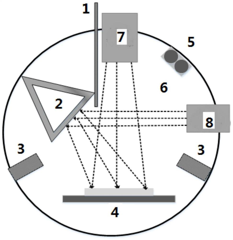
[0024] 1. Characterize the surface shape accuracy of the JGS1 substrate with a size of φ25.4×5mm, put it into an ion beam sputtering coating machine after cleaning and drying, set the single-layer film thickness to 500nm, and the coating material to be Ta 2 o 5 . The thin film deposition conditions are: the substrate temperature is 80°C, the method of reactive sputtering is adopted, the purity of the Ta target is 99.99%, and the vacuum is pumped to 8×10 -7 Torr.
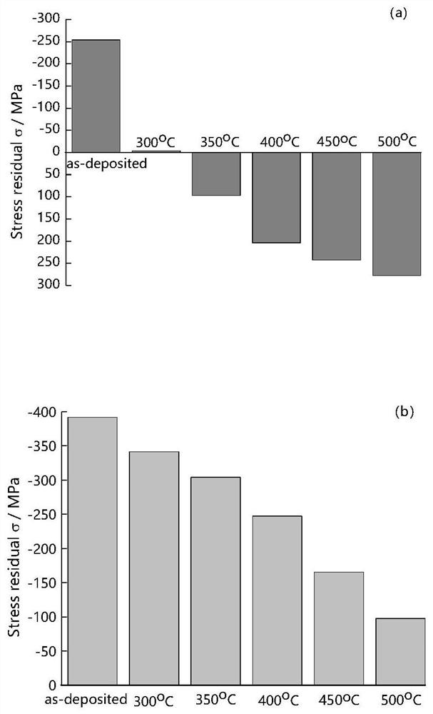
[0025] 2. To Ta 2 o 5 To characterize the surface shape accuracy of the thin film, its size is 0.018λ, and brought into Stoney formula (5), to get Ta 2 o 5 film stress.
[0026] The relationship among substrate diameter, sagittal height and radius of curvature can be expressed as:
[0027]
[0028] where R is the radius of curvature, D s is the diameter of the substrate, and h is the height of the arrow.
[0029] The relationship between Yagao an...
Embodiment 2
[0042] Example 2: SiO 2 Thin film stress properties
[0043] 1. Characterize the surface shape accuracy of the JGS1 substrate with a size of φ25.4×5mm, put it into an ion beam sputtering coating machine after cleaning and drying, set the single-layer film thickness to 500nm, and the coating material to be SiO 2 . The thin film deposition conditions are: the substrate temperature is 80°C, the method of reactive sputtering is adopted, the purity of the Si target is 99.99%, and the vacuum is pumped to 8×10- 7 Torr.
[0044] 2. On SiO 2 The surface shape accuracy of the thin film is characterized, and its size is 0.032λ, and it is brought into the Stoney formula (5). For the specific derivation process, refer to step (2) of Example 1 to obtain SiO 2 film stress.
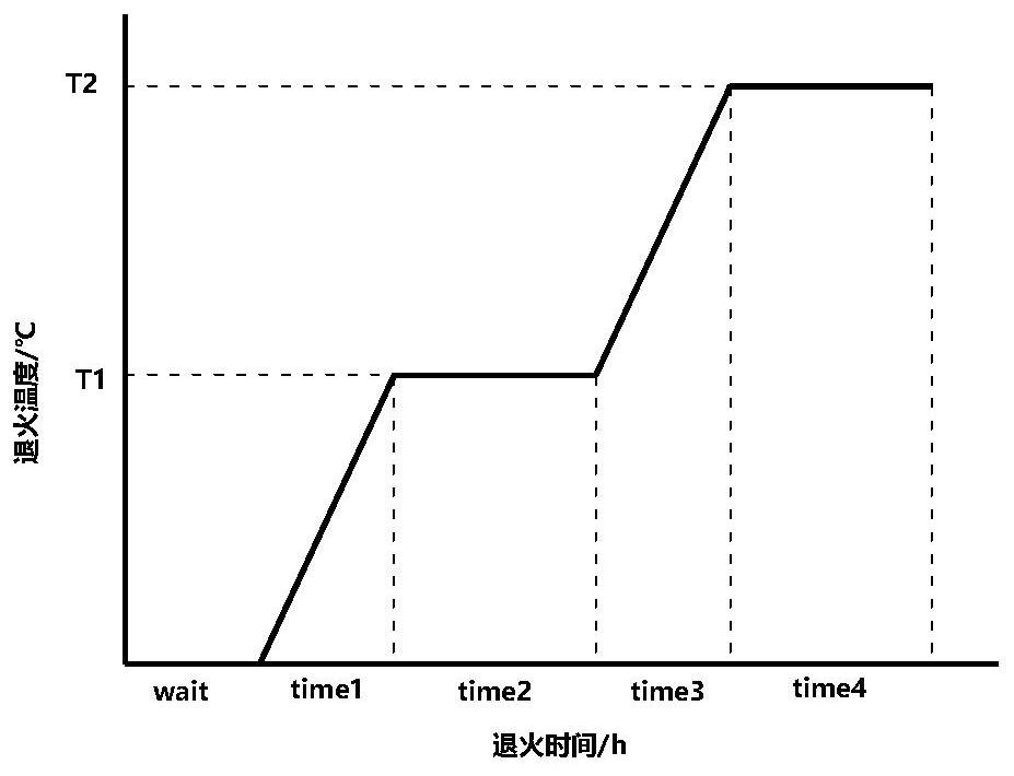
[0045] 3. On SiO 2 The annealing heat treatment was performed on the film. The annealing constant temperature was set at 80-600°C, the heating rate from room temperature to the annealing temperature was 100°C / h, an...
Embodiment 3
[0049] 1. According to relational formula (6) and (7) in embodiment 1 and 2, design multilayer film system is sub / HL ^16 / air, high and low refractive index coating materials are Ta 2 o 5 and SiO 2 , whose thicknesses are 197 nm and 115 nm, respectively.
[0050] Then, the surface shape accuracy of the JGS1 substrate with a size of φ25.4×5mm was characterized. After cleaning and drying, it was placed in an ion beam sputtering coating machine. The film deposition conditions were: the substrate temperature was 80°C, and the reactive sputtering method was used. The purity of the Ta target is 99.99%, vacuum pumped to 8×10 -7 Torr.
[0051] 2. Combining formulas (5), (6) and (7), the selected annealing temperature is 450 ° C, for Ta 2 o 5 / SiO 2 The multilayer film is annealed and heat-treated.
[0052] σ H (t H , T)t H +σ L (t L , T)t L =0 (4)
[0053] where t H , t L are the film thicknesses of high and low refractive index materials respectively, and T is the an...
PUM
| Property | Measurement | Unit |
|---|---|---|
| Thickness | aaaaa | aaaaa |
Abstract
Description
Claims
Application Information
PatSnap Eureka turns technology decisions into work you can execute. Powered by our Innovation Knowledge Graph, it runs expert workflows across engineering, life sciences, materials and intellectual property. Get your review-ready output in minutes.


