
Manufacturing method of ohmic contact electrode of optical communication chip

A technology of ohmic contact electrodes and manufacturing methods, which is applied in the manufacture of circuits, electrical components, and final products, and can solve the problems of semi-finished chip damage, reduced yield, and increased device resistance, achieving firm adhesion and reducing contact resistance Effect

Active Publication Date: 2021-06-18
湖北光安伦芯片有限公司
View PDF12 Cites 1 Cited by
  • Summary
  • Abstract
  • Description
  • Claims
  • Application Information

AI Technical Summary

Problems solved by technology

[0002] The production of metal ohmic contact electrodes is a key process in semiconductor manufacturing, especially in the optical communication chip manufacturing industry. The ohmic contact with low resistance and stable contact is the key factor affecting the performance and stability of the die. If the reliability of the ohmic contact resistance is poor , will increase the resistance value of the device, and in serious cases will directly cause the device to fail
[0003] In addition, in most conventional optical communication chip manufacturing processes, when it is impossible to make an ohmic contact electrode with the same cleavage region as the P surface on the N surface, the thickness of the ohmic contact electrode on the N surface restricts the cleavage effect
Although the thicker N-side ohmic contact electrode is beneficial to the heat dissipation of the chip and reduces the power consumption of the device, but the thicker N-side ohmic contact electrode is also easy to cause the N-side electrode adhesion after cleavage, which will directly lead to damage to the semi-finished chip and reduce the power consumption of the device. Yield

Method used


Image

  • Manufacturing method of ohmic contact electrode of optical communication chip

Examples


specific Embodiment

[0040] A specific embodiment of the manufacturing method of the optical communication chip ohmic contact electrode of the present invention is as follows:

[0041] On the surface of InP or GaAs substrate, quantum wells and active regions are grown by epitaxial technology, organic cleaning, plasma-enhanced chemical vapor deposition, and photolithography are used to make ridge photoresist patterns on the surface of the epitaxial layer, and reactive ion etching is used. , Wet etching technology transfers the ridge pattern to the epitaxial layer to produce a ridge structure; again uses plasma enhanced chemical vapor deposition, photolithography, and reactive ion etching technology to produce a passivation protection layer on the surface of the epitaxial layer, and the ridge structure The basic structure of the semiconductor optical communication chip such as the ohmic electrode contact area on the top of the strip, and the passivation protection layer adopts SiO2 or SiN;

[0042] ...


PUM

PropertyMeasurementUnit
Thicknessaaaaaaaaaa
Thicknessaaaaaaaaaa
Thicknessaaaaaaaaaa

Abstract

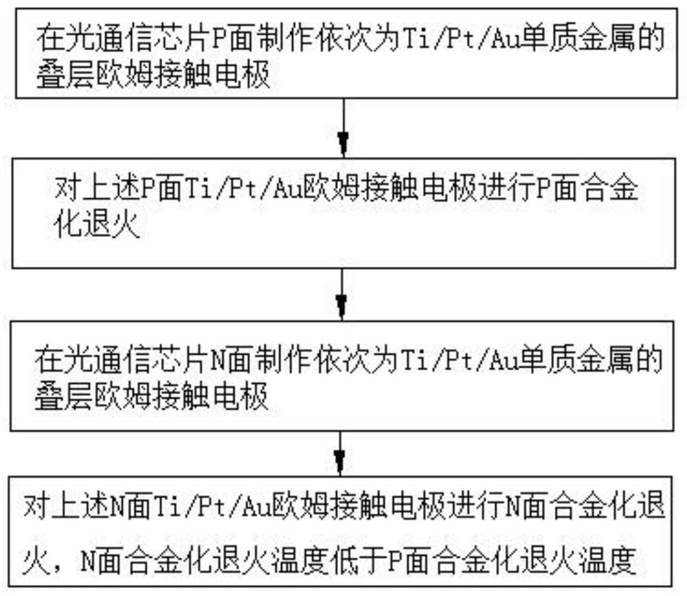
The invention relates to a manufacturing method of an ohmic contact electrode of an optical communication chip. The method comprises the following steps of: manufacturing a laminated ohmic contact electrode of Ti / Pt / Au elementary metal on a P surface of the optical communication chip; performing P-surface alloying annealing on the P-surface Ti / Pt / Au ohmic contact electrode, the P-surface alloying annealing temperature is T1; manufacturing a laminated ohmic contact electrode of Ti / Pt / Au elementary metal on the N surface of the optical communication chip; performing N-surface alloying annealing on the N-surface Ti / Pt / Au ohmic contact electrode, wherein the N-surface alloying annealing temperature is T2, and the P-surface alloying annealing temperature T1 is higher than the N-surface alloying annealing temperature T2. According to the ohmic contact electrode manufacturing process, the ohmic contact electrode stable in process and low in contact resistance can be obtained, and the optical communication chip stable in performance, excellent in chip appearance and high in yield is finally obtained by matching with the cleavage cutting process.

Description

technical field [0001] The invention belongs to the field of semiconductor manufacturing, and in particular relates to a method for manufacturing an ohmic contact electrode of an optical communication chip. Background technique [0002] The production of metal ohmic contact electrodes is a key process in semiconductor manufacturing, especially in the optical communication chip manufacturing industry. The ohmic contact with low resistance and stable contact is the key factor affecting the performance and stability of the die. If the reliability of the ohmic contact resistance is poor , will increase the resistance value of the device, and in serious cases will directly cause the device to fail. [0003] In addition, in most conventional optical communication chip manufacturing processes, when it is impossible to make ohmic contact electrodes with the same cleavage region as the P surface on the N surface, the thickness of the ohmic contact electrodes on the N surface restrict...

Claims


Application Information

Patent Timeline
IPC IPC(8): H01L31/0224H01L31/18H01L33/40H01L33/00
CPCH01L31/022408H01L31/1876H01L33/40H01L33/005Y02P70/50
Inventor 赵亮葛婷尹建峰
Owner 湖北光安伦芯片有限公司
Learn More