Infrared focal plane detector and manufacturing method thereof

A technology of an infrared focal plane and a manufacturing method, applied in the field of infrared focal plane detectors and their manufacturing, can solve the problems of signal attenuation, performance degradation of infrared detectors, crosstalk of photosensitive elements, etc., so as to reduce size, improve detection accuracy, and avoid crosstalk effect

Inactive Publication Date: 2021-06-22
北京智创芯源科技有限公司
View PDF1 Cites 0 Cited by
  • Summary
  • Abstract
  • Description
  • Claims
  • Application Information

AI Technical Summary

Problems solved by technology

[0003] In the preparation process of the existing mercury cadmium telluride infrared focal plane detector, after the injection junction process is completed, the size of the implanted area will have a certain lateral diffusion, and improper control will cause electrical connection between photosensitive elements (ie, detection pixels), resulting in The crosstalk between photosensitive elements is serious; in order to avoid crosstalk, the method of reducing the injection area is generally designed. In this case, it is easy to cause signal attenuation and cause the performance of the infrared detector to decline. Please refer to figure 1 , figure 1 It is a schematic diagram of the structure of the diffusion of the mercury cadmium telluride infrared detector when it is implanted.

Method used


Image

  • Infrared focal plane detector and manufacturing method thereof
  • Infrared focal plane detector and manufacturing method thereof
  • Infrared focal plane detector and manufacturing method thereof

Examples


specific Embodiment approach

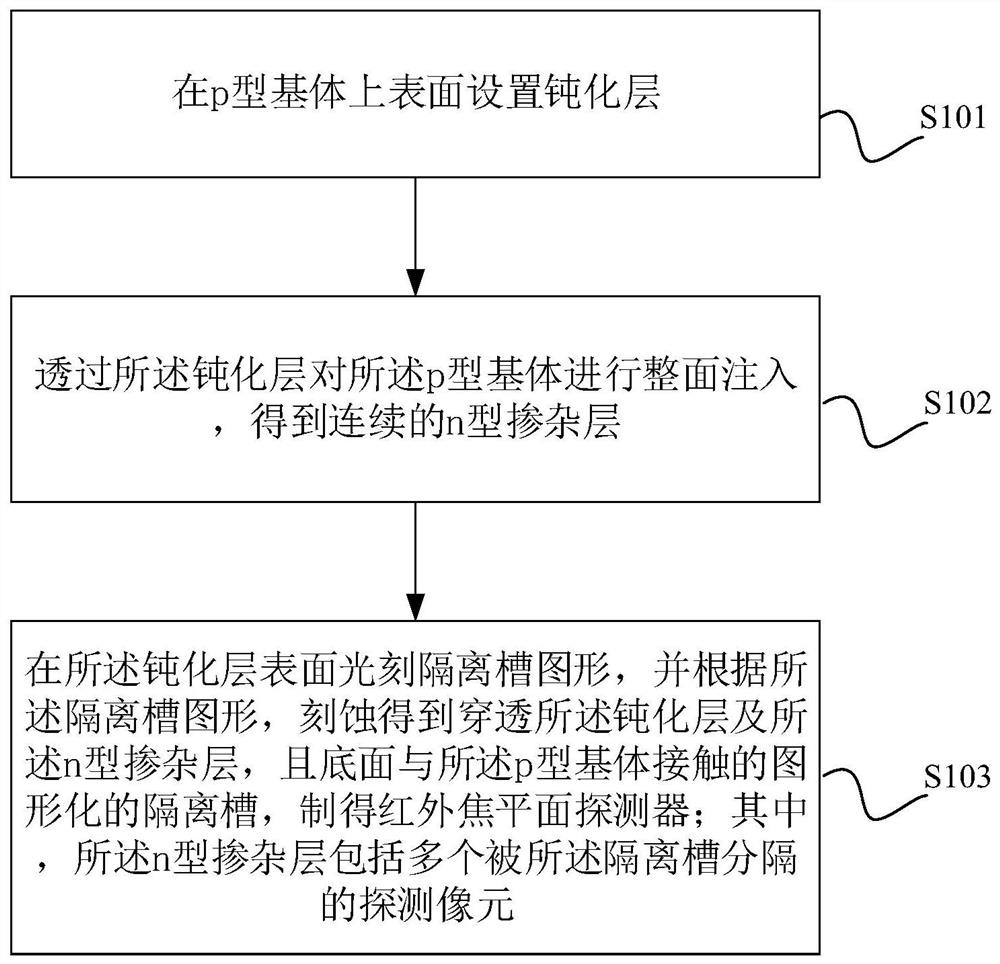
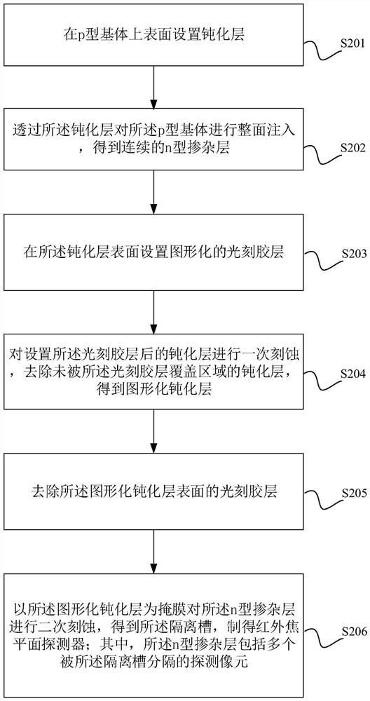
[0038] The core of the present invention is to provide a method for manufacturing an infrared focal plane detector, and a schematic flow chart of a specific implementation thereof is as follows: figure 2 As shown, it is called the first specific implementation mode, including:

[0039] S101: setting a passivation layer on the upper surface of the p-type substrate.

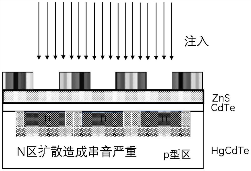
[0040] As a preferred embodiment, the p-type matrix is ​​a mercury cadmium telluride matrix, which is an important material for preparing infrared detectors. Due to its adjustable band gap, the detection spectrum ranges from short-wave bands to Extending to the very long wave band, it has the advantages of high photoelectric detection efficiency; correspondingly, the passivation layer is a zinc sulfide passivation layer.

[0041] Wherein, the zinc sulfide passivation layer has a thickness ranging from 0.2 microns to 0.5 microns, inclusive, such as any one of 0.20 microns, 0.30 microns or 0.50 microns.

[0042] S...

specific Embodiment approach 4

[0076] The present invention also provides a kind of infrared focal plane detector at the same time, the structure schematic diagram of a kind of specific embodiment of it is as follows Figure 6 As shown, it is called the fourth specific embodiment, which includes a p-type base 100, an n-type doped layer 200 and a passivation layer 400 from bottom to top;

[0077] The passivation layer 400 includes a patterned isolation groove 410;

[0078] The isolation groove 410 penetrates the passivation layer 400 and the n-type doped layer 200 , and its bottom surface is in contact with the p-type base 100 ;

[0079] The n-type doped layer 200 includes a plurality of detection pixels separated by the isolation groove 410 .

[0080] In addition, a passivation transition layer 300 is further included between the n-type doped layer 200 and the passivation layer 400 .

[0081] Taking the infrared focal plane detector of mercury cadmium telluride material described above as an example, the ...


PUM

PropertyMeasurementUnit
widthaaaaaaaaaa
thicknessaaaaaaaaaa
thicknessaaaaaaaaaa

Abstract

The invention discloses a manufacturing method of an infrared focal plane detector. The method comprises the following steps: arranging a passivation layer on the upper surface of a p-type substrate; performing whole-surface injection on the p-type substrate through the passivation layer to obtain a continuous n-type doped layer; photoetching an isolation groove pattern on the surface of the passivation layer, and etching according to the isolation groove pattern to obtain a patterned isolation groove which penetrates through the passivation layer and the n-type doping layer and of which the bottom surface is in contact with the p-type substrate, so as to prepare the infrared focal plane detector, wherein the n-type doped layer comprises a plurality of detection pixels which are separated by the isolation grooves. The adjacent detection pixels are spatially separated through the isolation grooves, the crosstalk phenomenon between the detection pixels is avoided, the detection precision of the detector is improved, the signal strength is guaranteed, ion implantation doping does not need to be carried out through a photoresist layer, and the problem of surface pollution residues before implantation is avoided. The invention also provides an infrared focal plane detector with the above beneficial effects.

Description

technical field [0001] The invention relates to the field of infrared detection, in particular to an infrared focal plane detector and a manufacturing method thereof. Background technique [0002] With the development of technology, infrared detectors are widely used in military and civil fields such as early warning detection, infrared reconnaissance, and imaging guidance. The preparation of infrared detector chips is the core of infrared detection technology. With the continuous development of infrared detector technology, the spacing of photosensitive elements of focal plane arrays is getting smaller and smaller, and the resolution and sensitivity are constantly improving. At the same time, along with the diffraction effect related to the detection target wavelength, the crosstalk phenomenon between pixels is also more obvious. A typical HgCdTe infrared detector manufacturing process usually uses a high-precision photolithography process combined with a planar implantati...

Claims


Application Information

Patent Timeline
Patent Type & Authority Applications(China)
IPC IPC(8): H01L27/146
CPCH01L27/1463H01L27/14632H01L27/14687
Inventor 不公告发明人
Owner 北京智创芯源科技有限公司
Why Eureka
Try Eureka