Solar cell manufacturing process and chained coating equipment
A technology for solar cells and manufacturing processes, applied in sustainable manufacturing/processing, final product manufacturing, circuits, etc., which can solve problems affecting cell yield, production efficiency and cost, inability to fully activate passivation capability, front surface contamination, etc. problems, to achieve the effect of improving yield and production efficiency, improving battery efficiency, and avoiding turnover
- Summary
- Abstract
- Description
- Claims
- Application Information
AI Technical Summary
Problems solved by technology
Method used
Image
Examples
Embodiment 1
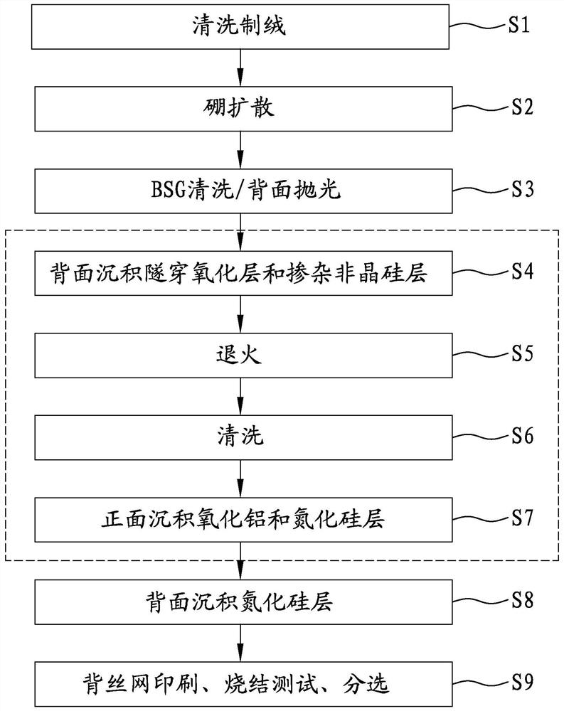
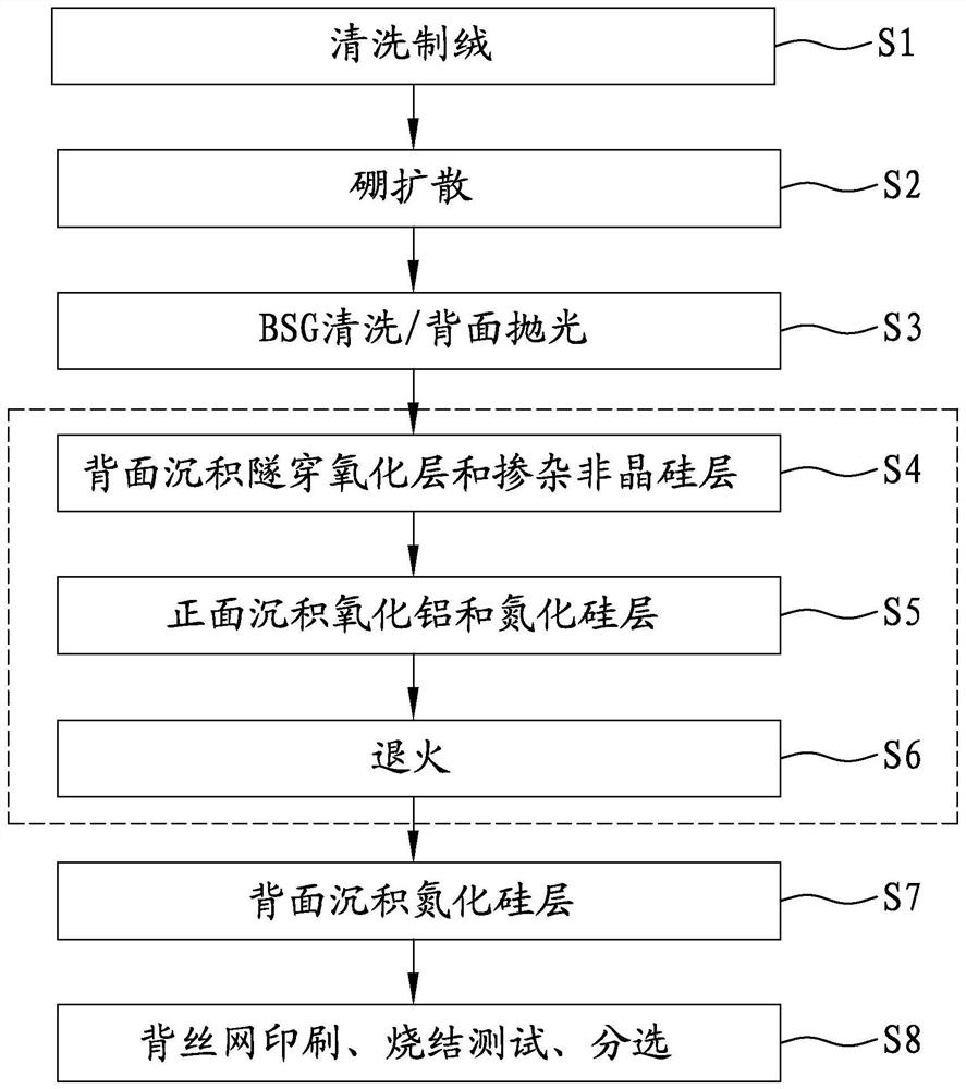
[0025] refer to figure 2 , the solar cell manufacturing process provided in this embodiment 1 includes the following steps:
[0026] S1. Select N-type crystalline silicon substrate, clean and texture the silicon substrate;
[0027] S2. Boron diffusion to prepare PN junction;
[0028] S3. Clean and remove the BSG layer, and perform backside polishing;
[0029] S4. A tunnel oxide layer with a thickness of 0.5-2nm is grown on the back of the N-type crystalline silicon substrate, and a doped amorphous silicon layer with a thickness of 20-200nm is deposited on the tunnel oxide layer;
[0030] S5. Prepare an aluminum oxide+silicon nitride stack on the front side of the N-type crystalline silicon substrate;
[0031] S6. Annealing, the annealing process temperature is 500-900°C, and the annealing time is 1-30min. High temperature is used to activate the doping atoms on the back of the N-type crystalline silicon substrate, so that the back of the N-type crystalline silicon is cryst...
Embodiment 2
[0037] The difference between the present embodiment 2 and the embodiment 1 is that the steps S4 and S5 in the embodiment 1 are sequentially exchanged in the present embodiment 2, namely:
[0038] S4. prepare an aluminum oxide+silicon nitride stack on the front side of the N-type crystalline silicon substrate;
[0039] S5. A tunnel oxide layer with a thickness of 0.5-2 nm is grown on the back of the N-type crystalline silicon substrate, and a doped amorphous silicon layer with a thickness of 20-200 nm is deposited on the tunnel oxide layer.
Embodiment 3
[0041] This Example 3 provides a TOPCon solar cell manufactured by using the solar cell manufacturing process described in Example 1 or 2.
PUM
| Property | Measurement | Unit |
|---|---|---|
| thickness | aaaaa | aaaaa |
| thickness | aaaaa | aaaaa |
Abstract
Description
Claims
Application Information
 - R&D
- Intellectual Property
- Life Sciences
- Materials
- Tech Scout
- Unparalleled Data Quality
- Higher Quality Content
- 60% Fewer Hallucinations
Browse by: Latest US Patents, China's latest patents, Technical Efficacy Thesaurus, Application Domain, Technology Topic, Popular Technical Reports.
© 2025 PatSnap. All rights reserved.Legal|Privacy policy|Modern Slavery Act Transparency Statement|Sitemap|About US| Contact US: help@patsnap.com


