Method for manufacturing circuit board by using remelting solder as weldable protective layer
A circuit board method and solderability technology, which is used in the assembly of printed circuits with electrical components, printed circuits, and printed circuit manufacturing. easy effect
- Summary
- Abstract
- Description
- Claims
- Application Information
AI Technical Summary
Problems solved by technology
Method used
Image
Examples
Embodiment 1
[0058] In this embodiment, a circuit board with pure thermosetting ink printed on both sides and fully cured is taken as an example. The specific steps are as follows:
[0059] (1) While using laser to remove the solder resist on the welding area to create a solder resist pattern, perform solderability treatment on the welding area.
[0060] After etching and stripping the film, for the manufacture of solder resist patterns of general precision and high precision circuit boards, the existing technology uses photosensitive solder resist materials, which require pre-baking, exposure, development, curing and other processes to obtain solder resist patterns. This step applies laser photoetching processing, which can directly vaporize and remove the solder resist material on the surface of the copper foil in the welding area, so there is no need to use photosensitive solder resist, and no pre-baking, exposure, development and other processes are required. After the solder resist is...
Embodiment 2
[0084] In this embodiment, a circuit board with PI laminated on both sides instead of solder resist ink is taken as an example. The specific steps are as follows:
[0085] (1) While using laser to remove the solder resist on the welding area to create a solder resist pattern, perform solderability treatment on the welding area.
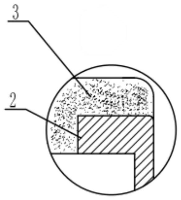
[0086] In this embodiment, the copper-clad substrate 1 is taken as an example, and the conductive circuit and the surface pad copper layer 2 have been laminated with PI as the solder resist 3, and then the solder resist 3 in the welding area is removed by laser to create a solder resist pattern. Solderability treatment is performed to expose a cleaned and solderability treated surface4. Such as Figure 1-4 shown.
[0087] Specifically, in this embodiment, the ultraviolet nanosecond laser machine U6 produced by Dezhong Technology Co., Ltd. is used to remove the PI in the welding area to make the solder resist pattern. The thickness of the PI layer is...
PUM
| Property | Measurement | Unit |
|---|---|---|
| Thickness | aaaaa | aaaaa |
| Thickness | aaaaa | aaaaa |
| Particle size | aaaaa | aaaaa |
Abstract
Description
Claims
Application Information
 - R&D Engineer
- R&D Manager
- IP Professional
- Industry Leading Data Capabilities
- Powerful AI technology
- Patent DNA Extraction
Browse by: Latest US Patents, China's latest patents, Technical Efficacy Thesaurus, Application Domain, Technology Topic, Popular Technical Reports.
© 2024 PatSnap. All rights reserved.Legal|Privacy policy|Modern Slavery Act Transparency Statement|Sitemap|About US| Contact US: help@patsnap.com


