

Microstructure glass substrate and preparation method thereof
A technology of glass substrate and microstructure, which is applied in the manufacture of final products, sustainable manufacturing/processing, electrical components, etc. It can solve the problems of affecting the efficiency of photon photoelectric emission materials, affecting the spectral sensitivity of photoelectric conversion, and the large difference in optical constants. , to achieve the effect of increasing spectral transmittance, improving spectral sensitivity, and increasing light transmittance
- Summary
- Abstract
- Description
- Claims
- Application Information
AI Technical Summary
Problems solved by technology
Method used
Image

Examples
preparation example Construction
[0076] An embodiment of the present invention also proposes a method for preparing a microstructured glass substrate, which includes the following steps:
[0077] (1) pretreating the glass base layer, the glass base layer comprising a photon incident surface and a photon exit surface;
[0078] The pretreatment includes: deionized water rolling brush, dish brush cleaning, ultrasonic cleaning, air drying, hot air drying.
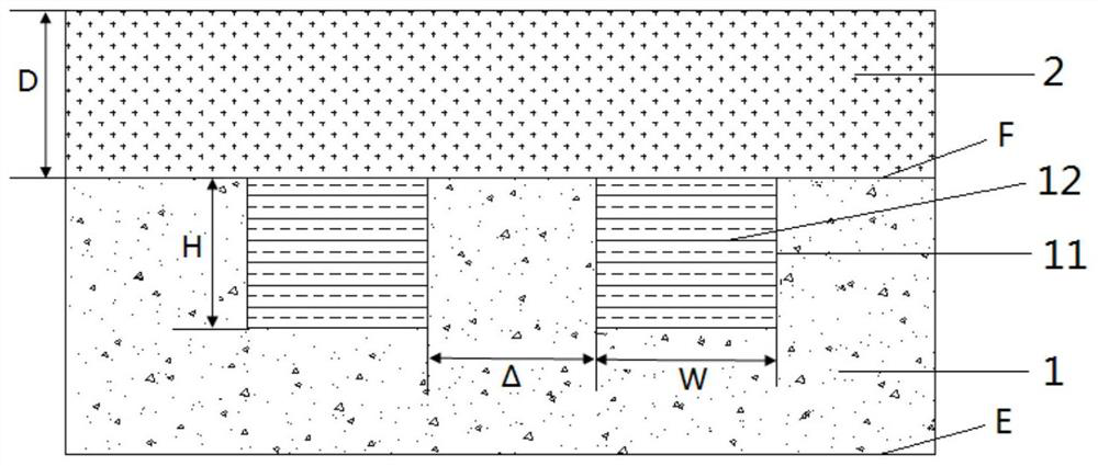
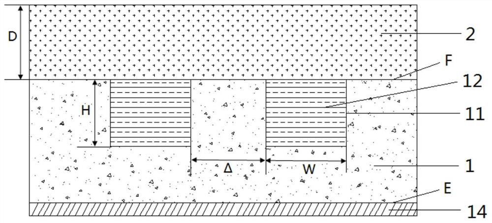
[0079] (2) In the direction extending from the photon exit surface to the photon incident surface, laser etching is carried out on the glass base layer, and several grooves in the first direction and some grooves in the second direction are etched out. The grooves cross each other to form a grating groove structure distributed in a grid pattern;
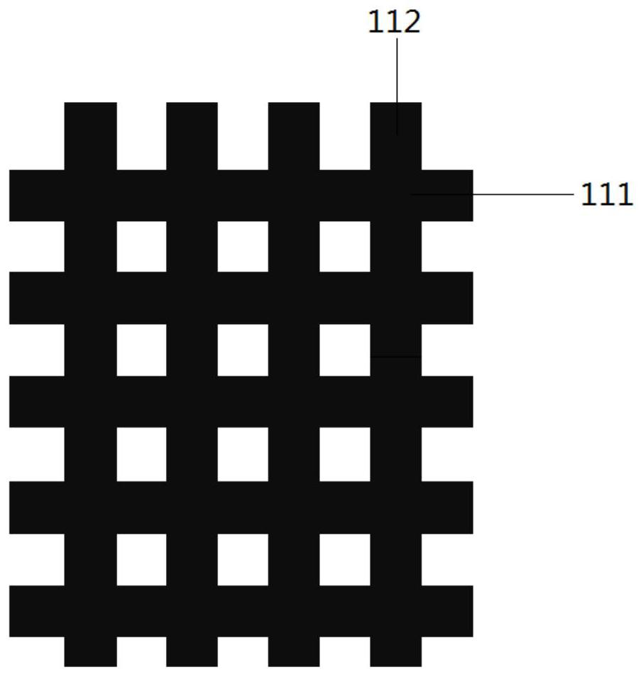
[0080] In some embodiments, the etching result of the grating groove structure is as follows image 3 As shown, the laser first marks the groove 111 in the first direction, and marks the groove 112 in the second di...
Embodiment 1
[0104] A method for preparing a microstructured glass substrate, specifically comprising the steps of:
[0105] (1) Pretreatment of the glass base layer: the square quartz glass base layer is cleaned by deionized water rolling brush, disk brush, ultrasonic cleaning, air drying, and hot air drying;
[0106] (2) Preparation of grating groove structure: In the direction extending from the photon exit surface to the photon incident surface, an infrared femtosecond laser is used for laser etching to draw lines on the square quartz glass substrate layer, firstly, along the first direction. Draw the groove in the first direction, and then draw the groove in the second direction according to the orthogonal direction. As shown in Figure 3, the filled part is the groove, and the blank part is the unmarked position; The depth, width and spacing are the same, wherein the groove width W=400nm, the spacing Δ=350nm, and the depth H=250-270nm; the laser etching and scribing adopts an infrared...
Embodiment 2
[0113] A method for preparing a microstructured glass substrate, specifically comprising the steps of:
[0114] (1) Pretreatment: the square quartz glass base layer is cleaned by deionized water rolling brush, disk brush, ultrasonic cleaning, air drying, and hot air drying;
[0115] (2) Preparation of SiO 2 Gradient refractive index coating: Alternately coat sol A and sol B on the photon incident surface of the pretreated square quartz glass substrate layer by dipping and pulling method, specifically, immerse in sol A first, and the pulling speed is 1mm / s, after the coating is complete, stand at 50°C for 10 minutes, then immerse in sol B, the pulling speed is 0.5mm / s, after the coating is complete, dip at 50°C for 10 minutes, so alternately. Each coating of A and B is a coating cycle. After 50 coating cycles, the quartz glass substrate layer is placed in an oven for heat treatment. The heat treatment steps and process play a decisive role in the gradual structure and adhesio...
PUM
| Property | Measurement | Unit |
|---|---|---|
| thickness | aaaaa | aaaaa |
| width | aaaaa | aaaaa |
| thickness | aaaaa | aaaaa |
Abstract
Description
Claims
Application Information