

Ga-GaSb nano material and preparation method thereof
A nanomaterial and solution technology, applied in nanotechnology, nanotechnology, chemical instruments and methods, etc., can solve problems such as unfavorable large-scale production development, in-depth GaSb, and limited application.
- Summary
- Abstract
- Description
- Claims
- Application Information
AI Technical Summary
Problems solved by technology
Method used
Image

Examples
preparation example Construction
[0047] The invention provides a preparation method of Ga-GaSb nanometer material, comprising:
[0048] Trimethylaminogallium dimer and triphenylantimony react in octadecene to form Ga-GaSb nanomaterials.
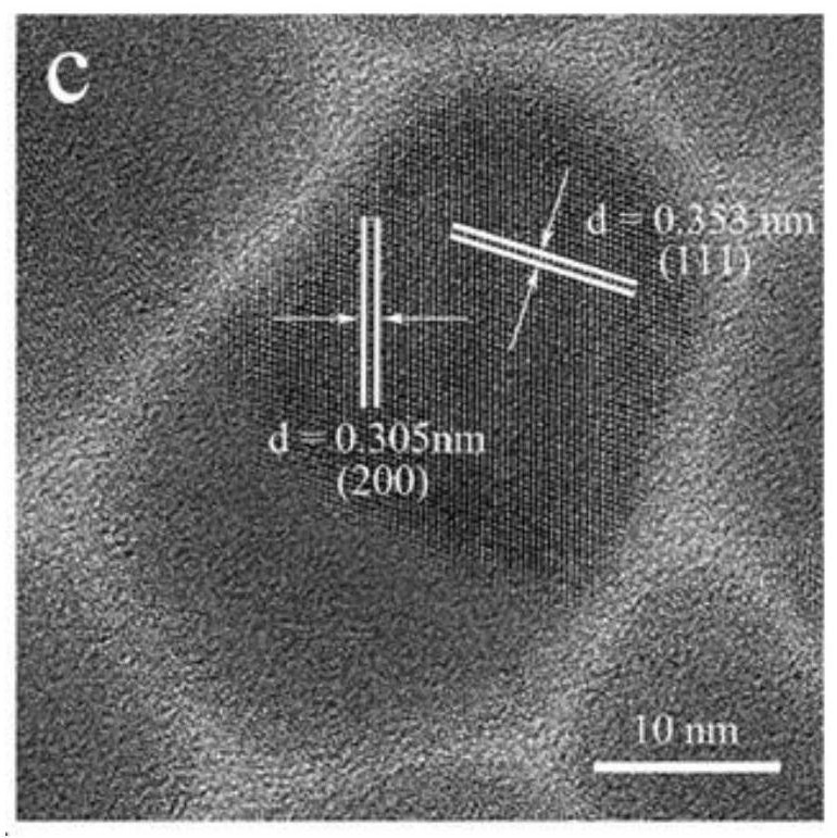
[0049] The preparation method provided by the invention is a solution-phase synthesis method, with specific organic gallium source-trimethylaminogallium dimer (C 12 h 36 Ga 2 N 6 ) and organic antimony source - triphenyl antimony (Sb(Ph) 3) is used as a precursor to react in a specific reaction medium octadecene, and Ga-GaSb nanomaterials can be synthesized by one-step heating, and the obtained materials have high dispersion and high purity. In the above reaction system, no catalyst is used, and the reaction is promoted by self-catalysis, and the above reaction greatly reduces the reaction temperature and reaction time. That is, the preparation method provided by the present invention greatly reduces the synthesis temperature and time under the premise of ensuring the h...
Embodiment 1
[0081] 1. Sample preparation:
[0082] S1. Add 10 mL of octadecene into a 100 mL three-necked flask for later use.
[0083] S2. Weigh 0.05 mmol (0.0176 g) of triphenyl antimony and 2.0 mL of octadecene into a beaker for ultrasonic dissolution with an ultrasonic power of 190 W for 2 min to obtain a triphenyl antimony solution.
[0084] S3. Transfer the obtained triphenylantimony solution to the above-mentioned three-necked flask filled with octadecene, and perform ultrasonic mixing at a power of 190W for 2 minutes. Afterwards, under the stirring of a high-temperature stirring magnet and in a reaction atmosphere of high-purity argon, the temperature was raised to 110° C. for 40 minutes to remove moisture and low-boiling impurities to obtain a mixed solution.
[0085] S4. While performing step S3, 0.075 mmol (0.0302 g) of trimethylaminogallium dimer was ultrasonically dissolved in 2.0 mL of dried octadecene, the ultrasonic power was 190 W, and the time was 2 min. It is then pla...
Embodiment 2~7
[0100] 1. Sample preparation:
[0101] According to the preparation process of Example 1, the difference is that in step S5, the reaction time is 1 min, 3 min, 5 min, 10 min, 15 min and 30 min respectively.
[0102] 2. Sample test:
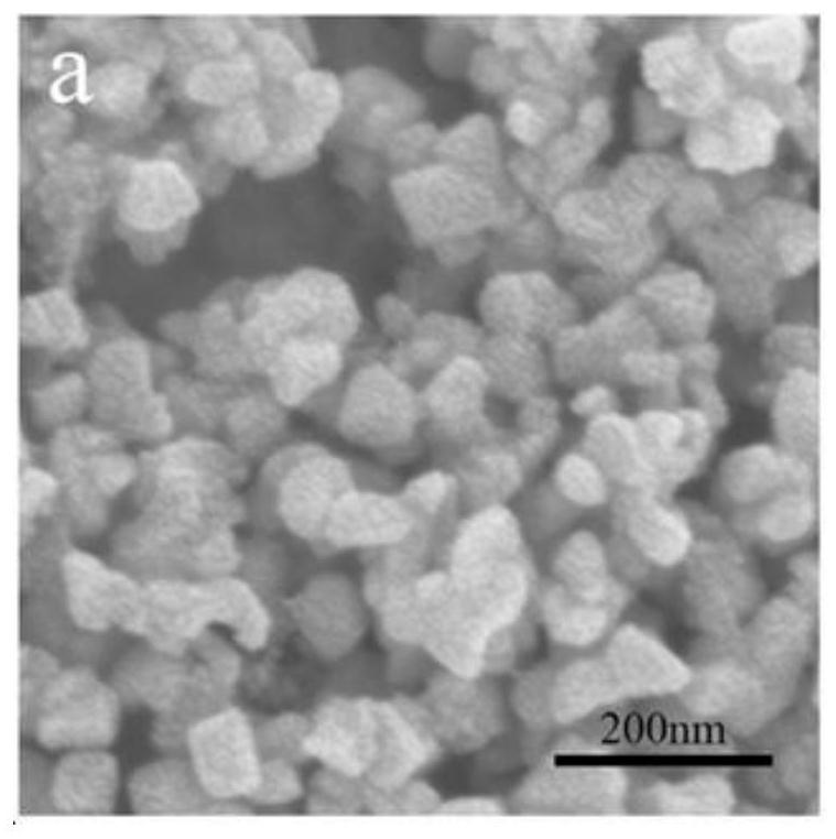
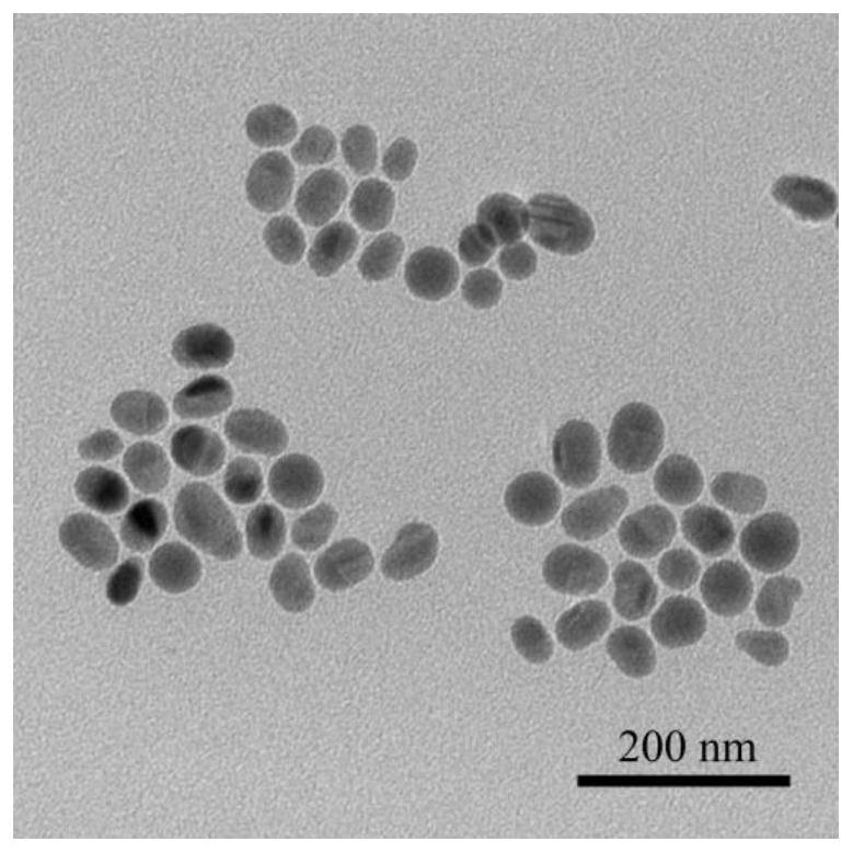
[0103] Gained material is carried out transmission electron microscope (TEM) test respectively, the result is respectively as follows Figure 10-16 as shown, Figure 10 It is the TEM figure of the gained Ga-GaSb nanometer material of embodiment 2 reaction 1min, Figure 11 It is the TEM figure of embodiment 3 reaction 3min gained Ga-GaSb nano material, Figure 12 It is the TEM figure of embodiment 4 reaction 5min gained Ga-GaSb nanometer material, Figure 13 It is the TEM figure of embodiment 5 reaction 10min gained Ga-GaSb nano material, Figure 14 It is the TEM figure of embodiment 6 reaction 15min gained Ga-GaSb nano material, Figure 15 It is the TEM picture of the Ga-GaSb nanomaterial obtained by reacting for 30 minutes in Example 7. De...
PUM
| Property | Measurement | Unit |
|---|---|---|
| diameter | aaaaa | aaaaa |
| length | aaaaa | aaaaa |
Abstract
Description
Claims
Application Information