Grating coupling structure based on back process and preparation method
A technology of grating coupling and grating structure, which is applied in the waveguide grating coupling structure, grating coupling structure and corresponding preparation fields, can solve the problems of limited compatibility and scalability, metal mirror process pollution, etc., and achieve maximum compatibility and reliability Expansibility, good consistency, and the effect of reducing coupling loss
- Summary
- Abstract
- Description
- Claims
- Application Information
AI Technical Summary
Problems solved by technology
Method used
Image

Examples
Embodiment 1
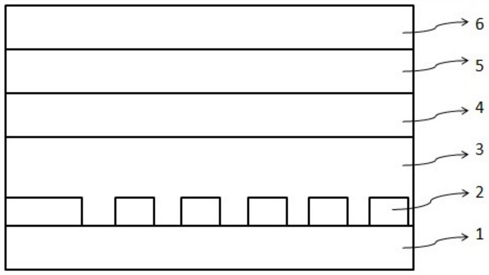
[0038]In Embodiment 1 of the present invention, a grating coupling structure based on a back-facing process is provided, including: a first transition layer, a waveguide diffraction grating layer, a second transition layer, a mirror layer, a third transition layer and The carrier sheet; the second transition layer covers the waveguide diffraction grating layer and is connected with the first transition layer; the reflection mirror layer is a non-metal structure, and the projection covers the waveguide diffraction grating layer.
[0039] Such as figure 1 As shown, the structure of the grating coupling structure from bottom to top is the first transition layer 1 , the waveguide diffraction grating layer 2 , the second transition layer 3 , the mirror layer 4 , the third transition layer 5 and the carrier 6 .
[0040] In the embodiment of the present invention, a grating coupling structure based on a back-to-back process is provided on the waveguide diffraction grating layer 2 wit...
Embodiment 2
[0042] Embodiment 2 is an example of the material and thickness range of each layer in the grating coupling structure, still refer to figure 1 , the material of the first transition layer 1, the second transition layer 3, and the third transition layer 5 is SiO 2 The thickness of the first transition layer 1 is less than 10 μm, the thickness of the waveguide diffraction grating layer 2 is less than 1 μm, and the thickness of the second transition layer 3 is in the range of 0-10 μm; the thickness of the first transition layer 1 is greater than the thickness of the waveguide diffraction grating layer 2; The thickness of the second transition layer 3 depends on the height of reflection enhancement according to the design requirements; the thickness selection range of the third transition layer 5 only needs to meet the requirements of the bonding process.
[0043] In this embodiment, the exemplary thickness of the first transition layer 1 is 2 μm; the exemplary thickness of the wa...
Embodiment 3
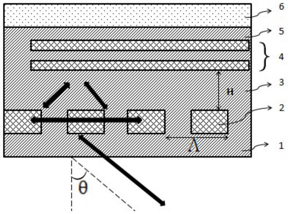
[0045] In embodiment three, refer to figure 2 , the mirror layer 4 is composed of a distributed Bragg reflector structure (DBR, Distributed Bragg Reflector) based on a multilayer dielectric film. The DBR structure is specifically a periodic structure composed of two materials with different refractive indices arranged alternately. Dielectric layer materials commonly used in existing processes Si, Si 3 N 4 According to the reflection wavelength and the refractive index of the dielectric film, the thickness of the dielectric film layer can be reasonably designed to achieve the effect of reflection enhancement.
[0046] The physical thickness of each dielectric film layer of the distributed Bragg reflector structure is recorded as t to satisfy: ,in is the central wavelength, is the effective refractive index of each dielectric layer; the total thickness of the DBR structure in this embodiment is less than 2 μm.
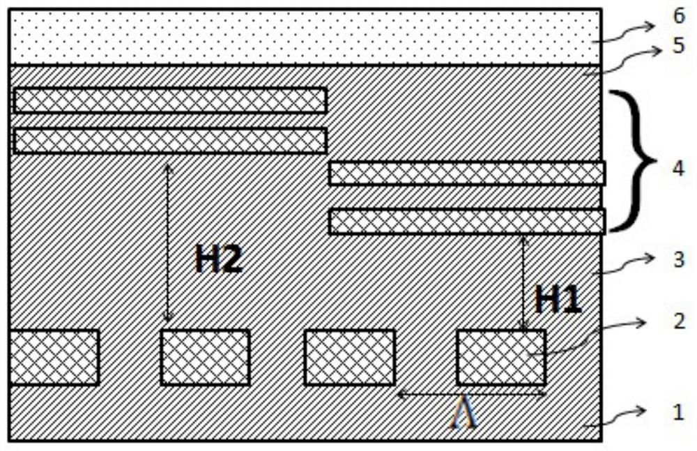
[0047] Such as figure 2 As shown, there are first transi...
PUM
| Property | Measurement | Unit |
|---|---|---|
| thickness | aaaaa | aaaaa |
| thickness | aaaaa | aaaaa |
| thickness | aaaaa | aaaaa |
Abstract
Description
Claims
Application Information
 - R&D Engineer
- R&D Manager
- IP Professional
- Industry Leading Data Capabilities
- Powerful AI technology
- Patent DNA Extraction
Browse by: Latest US Patents, China's latest patents, Technical Efficacy Thesaurus, Application Domain, Technology Topic.
© 2024 PatSnap. All rights reserved.Legal|Privacy policy|Modern Slavery Act Transparency Statement|Sitemap