Bidirectional transient voltage suppression device and preparation method thereof

A transient voltage suppression and device technology, applied in semiconductor/solid-state device manufacturing, electrical solid-state devices, electrical components, etc., can solve problems such as low clamping voltage and low breakdown voltage

Active Publication Date: 2021-09-10
SHANGHAI CHANGYUAN WAYON MICROELECTRONICS
View PDF4 Cites 2 Cited by
  • Summary
  • Abstract
  • Description
  • Claims
  • Application Information

AI Technical Summary

Problems solved by technology

[0004] At present, with the rapid development of microelectronics technology, integrated circuits continue to develop in the direction of low voltage, low power consumption, and high-speed transmission, and higher performance requirements are put forward for corresponding TVS protection devices, requiring TVS to have lower shock Breakthrough voltage and lower clamping voltage, while TVS using traditional technology has the problem of being difficult to continue to reduce the breakdown voltage, and its clamping voltage is still high, which still poses a considerable risk to the safe operation of subsequent integrated circuits

Method used


Image

  • Bidirectional transient voltage suppression device and preparation method thereof
  • Bidirectional transient voltage suppression device and preparation method thereof
  • Bidirectional transient voltage suppression device and preparation method thereof

Examples


Embodiment 1

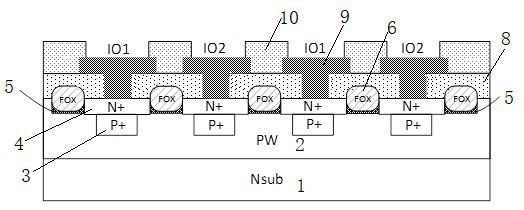
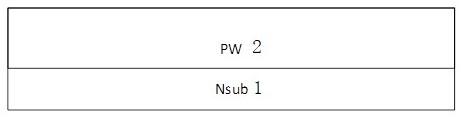
[0042] In a preferred embodiment of the present application, based on the above-mentioned problems existing in the prior art, a bidirectional transient voltage suppression device is now provided, such as Figure 1-11As shown, it includes: a substrate 1, the substrate 1 has a first conductivity type; a well region 2 is formed on the upper surface of the substrate 1, and the well region 2 has a second conductivity type; if the first conductivity type is N type , then the second conductivity type is P-type; if the first conductivity type is P-type, then the second conductivity type is N-type. In Embodiment 1, the first conductivity type is N-type, and the second conductivity type is P-type as an example. , that is, the substrate 1 is an N-type silicon chip N sub, and the well region 2 is a P-type PW; a first predetermined region is located in the well region 2, and the first predetermined region includes a plurality of first predetermined regions having a second conductivity type ...

Embodiment 2

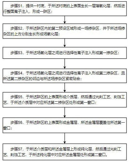
[0051] The present invention also provides a method for preparing a bidirectional transient voltage suppression device, which is used to prepare a bidirectional transient voltage suppression device as described above, such as figure 2 As shown, the following steps are also included: step S1, such as image 3 As shown, a substrate 1 (Nsub) is provided, a thin oxide layer is grown on the upper surface of the substrate 1 (Nsub), and then ion implantation is performed on the entire surface, and then a thermal process is carried out to form a well region 2 (PW) ; Preferably, the substrate 1 (Nsub) is N-type lightly doped, and the resistivity of the substrate 1 (Nsub) is 10~50Ω*cm; the growth thickness of the thin oxide layer is 200~500Å.

[0052] As a preferred implementation, in step S1, the ion implantation element in the well region 2 (PW) is boron or boron difluoride, the implantation energy is 60~100KeV, and the implantation dose is 2E12~1E13c , the implantation angle is 7 ...

Embodiment 3

[0072] Such as Figure 11 As shown, this embodiment is similar to Embodiment 2, the difference is that the doping type is changed, that is, the substrate 1 is changed from Nsub to Psub, the well region 2 is changed from PW to NW, and the first doped region 3 is changed from P+ to N+ , the second doped region 4 is changed from N+ to P+, and the field oxide layer 6 is changed from PF to NF. The other structures are the same as those in Embodiment 2, the manufacturing process is also the same, and the functions realized by the device remain unchanged.

[0073] The beneficial effect of the technical solution of the present invention is that the device prepared in the present invention has the characteristics of low breakdown voltage and larger negative resistance characteristics, so it has lower clamping voltage, and thus has ultra-low trigger voltage and ultra-low clamping voltage. The characteristics of the bit voltage, the ability to protect the subsequent circuit is stronger. ...


PUM

PropertyMeasurementUnit
thicknessaaaaaaaaaa
thicknessaaaaaaaaaa
thicknessaaaaaaaaaa

Abstract

The invention discloses a bidirectional transient voltage suppression device and a preparation method thereof, which belong to the field of semiconductor protection devices. Thebidirectional transient voltage suppression device comprises a substrate and a well region. The well region comprises a first preset region and a second preset region, and the first preset region comprises first doped regions arranged at intervals; the second preset region comprises field doped regions which are arranged in the well region at intervals andsecond doped regions. The second doped regions are arranged between the field doped regions, the adjacent sides of the second doped regions are tightly attached to the field doped regions, and the second doped regions are located on the upper surfaces of the first doped regions respectively; the field oxide layer is formed in the field doped region and protrudes out of the field dopedregion. The technical scheme of the invention has the beneficial effects that the characteristics of low breakdown voltage and higher negative resistance characteristic are simultaneously realized, so that the characteristics of lower clamping voltage, ultralow trigger voltage and ultralow clamping voltage are realized, and the capability of protecting a post-stage circuit is higher.

Description

technical field [0001] The invention relates to the field of semiconductor protection devices, in particular to a bidirectional transient voltage suppression device and a preparation method thereof. Background technique [0002] Transient Voltage Suppressor (TVS) is a high-efficiency clamp overvoltage protection device in the form of a diode. When the two poles of the TVS diode are impacted by reverse transient high energy, it can change the high impedance between its two poles to low impedance at a speed of 10 minus 12 seconds, absorbing surge power up to several thousand watts , so that the voltage between the two poles is clamped at a predetermined value, and the predetermined value is at a relatively low voltage level, so that the post-stage integrated circuit is protected from the impact of electrostatic discharge or surge voltage, and effectively protects the precision components in the electronic circuit , free from damage from various surge pulses. [0003] TVS dev...

Claims


Application Information

Patent Timeline
Patent Type & Authority Applications(China)
IPC IPC(8): H01L27/02H01L27/06H01L21/8222
CPCH01L27/0255H01L27/0647H01L21/8222
Inventor 蒋骞苑赵德益吕海凤霍田佳严林周凯彭阳
Owner SHANGHAI CHANGYUAN WAYON MICROELECTRONICS
Why Eureka
Try Eureka