

hemt device and its self-isolation method and manufacturing method
A technology of devices and conditions, applied in semiconductor/solid-state device manufacturing, semiconductor devices, electrical components, etc., can solve problems affecting device dynamic characteristics, deep energy level defects, device surface leakage, etc., to avoid collapse effect and reduce process complexity Degree and manufacturing cost, the effect of increasing the breakdown voltage
Active Publication Date: 2022-05-31
NINGBO INST OF MATERIALS TECH & ENG CHINESE ACADEMY OF SCI
View PDF8 Cites 0 Cited by
- Summary
- Abstract
- Description
- Claims
- Application Information
AI Technical Summary
Problems solved by technology
However, mesa etching is easy to introduce a large number of acceptor-like defects and surface states on the surface of the isolation region and the mesa, resulting in serious device surface leakage. In addition, mesa etching is non-planar isolation, and the gate electrode directly contacts the exposed 2DEG on the side wall of the mesa. Create an additional leakage channel
Ion implantation isolation mainly achieves the purpose of device isolation by forming high-resistance regions through high-energy ion implantation. Although this isolation method is a planar isolation structure, it will introduce deep-level defects and affect the dynamic characteristics of the device. It can be seen that traditional isolation There are many disadvantages in the technology, and new structures and new technologies need to be adopted to improve isolation efficiency and reduce device power consumption
Method used
View moreImage
Smart ImageViewing Examples

Examples
Embodiment 1
[0092] 4) A SiN surface passivation layer is deposited on the metal polar region, and a gate electrode is deposited on the SiN surface passivation layer.
Embodiment 2
[0099] 4) A SiN surface passivation layer is deposited in the nitrogen polar region, and a gate electrode is deposited on the SiN surface passivation layer.
[0103]
Embodiment 3
[0109] 4) depositing a SiN surface passivation layer on the metal polar region, and depositing a gate electrode on the SiN surface passivation layer.
Login to View More PUM
| Property | Measurement | Unit |
|---|---|---|
| thickness | aaaaa | aaaaa |
Abstract
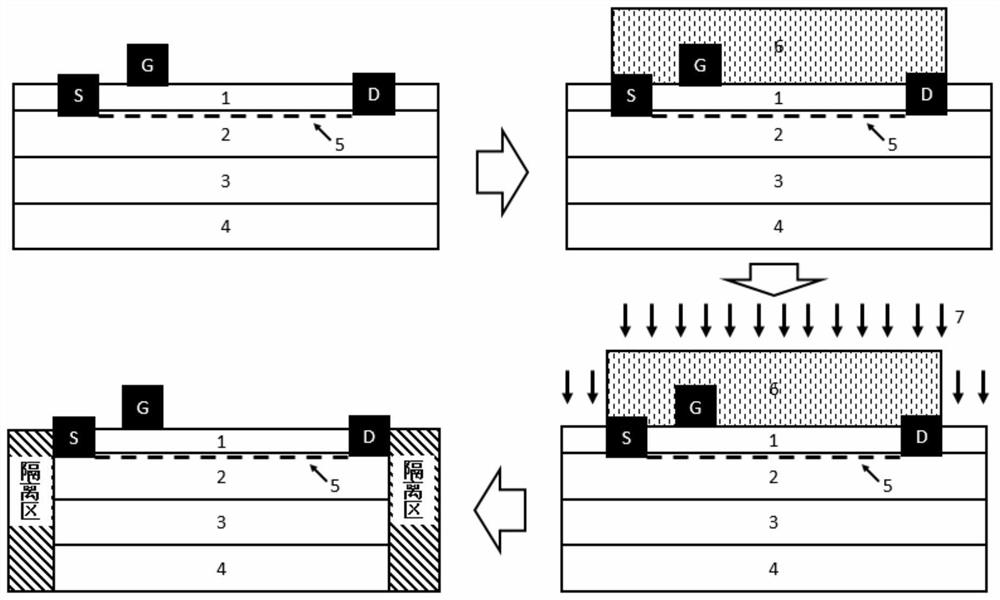
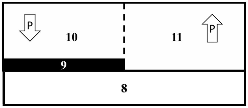
The invention discloses a HEMT device, a self-isolation method and a manufacturing method thereof. The self-isolation method includes: epitaxially growing an epitaxial layer with a lateral polar structure on a substrate with a patterned low-temperature crystallization layer on the surface, and adjusting the epitaxial growth conditions to make the surface of the formed metal polar region and the nitrogen polarity There is a set height difference between the surfaces of the regions, so that the two-dimensional electron gas or the two-dimensional hole gas formed in any one of the metal polar region and the nitrogen polar region is blocked by the other, which Either is used to fabricate HEMT bulk structures. An isolation method for a HEMT device provided by an embodiment of the present invention realizes isolation synchronously when the growth of the epitaxial structure is completed, without additional processes such as photolithography, plasma etching, or ion beam implantation.
Description
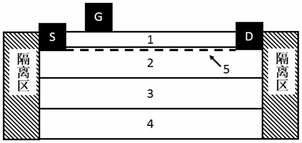
HEMT device, self-isolation method and fabrication method thereof technical field The present invention relates to a kind of isolation method of HEMT device, particularly a kind of HEMT device and self-isolation method thereof, The manufacturing method belongs to the technical field of semiconductors. Background technique [0002] High electron mobility transistors (HEMTs) based on GaN / AlGaN heterojunctions are expected to replace traditional silicon-based devices. Low-energy-loss power conversion and signal transmission under high-frequency and high-power working conditions, thus enabling high-speed rail and new energy vehicles It has been widely used in the fields of rate control units, smart grid chips, and microwave radio frequency front-ends for 5G. depletion HEMT Taking the device as an example, its schematic diagram is shown in Figure 1, which is mainly composed of a barrier layer 1, a channel layer 2, a buffer layer 3, and a substrate 4 [S.Wienecke,B.Romancz...
Claims
Login to View More Application Information
Patent Timeline
 Patent Type & AuthorityPatents(China)
IPC IPC(8): H01L21/335H01L29/06H01L29/778
CPCH01L29/66462H01L29/7781H01L29/0642H01L29/0684
Inventor郭炜叶继春戴贻钧徐厚强
OwnerNINGBO INST OF MATERIALS TECH & ENG CHINESE ACADEMY OF SCI