Preparation process of silicon substrate on power insulator

A preparation process and insulator technology, which is applied in the field of integrated circuit material preparation, can solve the problem of difficulty in accurately controlling the thickness uniformity of the silicon layer of the top device, etc.

Active Publication Date: 2021-09-21
ZHONGHUAN ADVANCED SEMICON MATERIALS CO LTD
View PDF3 Cites 2 Cited by
  • Summary
  • Abstract
  • Description
  • Claims
  • Application Information

AI Technical Summary

Problems solved by technology

However, due to the thinning process, it is difficult to precisely control the thickness uniformity of the top device silicon layer

Method used


Image

  • Preparation process of silicon substrate on power insulator
  • Preparation process of silicon substrate on power insulator
  • Preparation process of silicon substrate on power insulator

Examples


Embodiment Construction

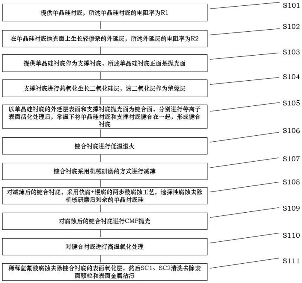
[0036] The specific implementation of the method for preparing a silicon-on-insulator substrate provided by the present invention will be described in detail below in conjunction with the accompanying drawings.

[0037] figure 1 Shown is the flow chart of the implementation steps of this specific embodiment, a preparation process of a silicon substrate on a power insulator, including the following steps:

[0038] Step S101, providing a single crystal silicon substrate, the single crystal silicon substrate is a heavily doped substrate with a resistivity of R1;

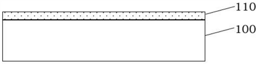
[0039] Step S102, growing a lightly doped single crystal epitaxial silicon layer on the surface of the single crystal silicon substrate, the epitaxial silicon layer has the same doping type as the single crystal silicon substrate, and the resistivity of the epitaxial silicon layer is R2;

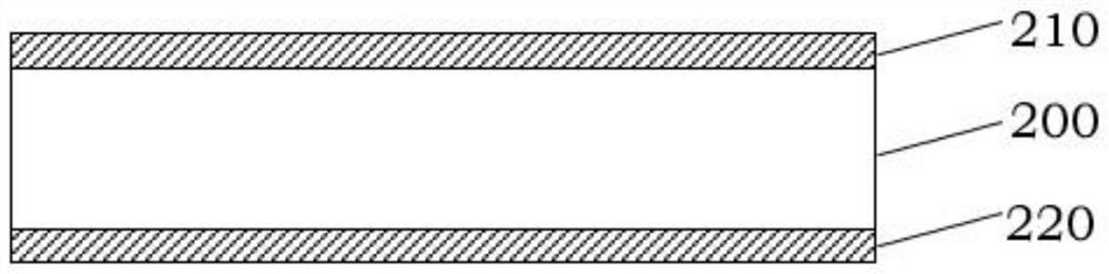
[0040] Step S103, providing a support substrate, the front surface of the support substrate is a polished surface;

[0041] Step S...


PUM


Abstract

The invention relates to a preparation process of a silicon substrate on a power insulator. The preparation process comprises the following steps: preparing a silicon epitaxial wafer as a device layer silicon substrate and an oxidized silicon wafer as a supporting silicon substrate, performing plasma surface activation treatment, performing low-temperature annealing after normal-temperature bonding, and performing low-temperature annealing after adopting a mechanical grinding thinning mode, removing a silicon single crystal of the substrate by using two-step selective acid corrosion of fast corrosion and slow corrosion, carrying out CMP polishing treatment, then carrying out high-temperature oxidation thinning treatment, and finally removing silicon oxide grown by high-temperature oxidation through diluted hydrofluoric acid corrosion; enabling the low-temperature annealing temperature after bonding to not exceed 400 DEG C; and enabling the polishing removal amount of the bonding wafer to not exceed 1 micron and the temperature of high-temperature oxidation annealing to not lower than 900 DEG C, and finally, obtaining the required silicon-on-insulator substrate after a surface oxide layer is removed through a wet cleaning process. The thickness and the uniformity of the silicon substrate device layer on the power insulator are accurately controlled in a thinning mode of selective corrosion and CMP polishing and high-temperature thermal oxidation.

Description

technical field [0001] The invention relates to a method for preparing integrated circuit materials, in particular to a method for preparing a silicon substrate on a power insulator. Background technique [0002] Semiconductor devices based on silicon-on-insulator (SOI) substrates have attracted much attention because of their obvious advantages in power consumption, operating speed, radiation resistance and device integration. In recent years, with the continuous improvement of process technology, the preparation of SOI materials has been rapidly developed. According to the thickness of the top silicon layer, SOI materials can be divided into thin film SOI (top silicon is usually less than 1 μm) and thick film SOI (top silicon is usually greater than 1 μm). The corresponding SOI product applications can be divided into radio frequency SOI, power SOI, image SOI and MEMS micro-electromechanical SOI and other categories; the main driving force of the thin-film SOI market come...

Claims


Application Information

Patent Timeline
Patent Type & Authority Applications(China)
IPC IPC(8): H01L21/762H01L21/306H01L21/324H01L21/02H01L21/304H01L21/67
CPCH01L21/76251H01L21/02164H01L21/02238H01L21/02255H01L21/0234H01L21/324H01L21/304H01L21/30608H01L21/67253
Inventor 马乾志孙晨光王彦君
Owner ZHONGHUAN ADVANCED SEMICON MATERIALS CO LTD
Why Eureka
Try Eureka