Three-dimensional hybrid multiplexing signal all-optical wavelength conversion device on silicon substrate

An all-optical wavelength conversion and three-dimensional hybrid technology, applied in the field of optical waveguides, to achieve the effects of simple structure, high conversion efficiency, and improved flexibility

Active Publication Date: 2021-10-08
ZHEJIANG UNIV
View PDF6 Cites 4 Cited by
  • Summary
  • Abstract
  • Description
  • Claims
  • Application Information

AI Technical Summary

Problems solved by technology

However, this device can only realize the wavelength conversion of the transverse electric mode of the signal, and usually requires the cooperation of the polarization controller and the coupling grating of the transverse electric mode.
Therefore, the prior art lacks an all-optical wavelength conversion method that is suitable for polarization multiplexing signals, wavelength division multiplexing signals and mode multiplexing signals and has high broadband efficiency

Method used


Image

  • Three-dimensional hybrid multiplexing signal all-optical wavelength conversion device on silicon substrate
  • Three-dimensional hybrid multiplexing signal all-optical wavelength conversion device on silicon substrate
  • Three-dimensional hybrid multiplexing signal all-optical wavelength conversion device on silicon substrate

Examples


Embodiment Construction

[0035] The present invention will be further described below in conjunction with the accompanying drawings and embodiments.

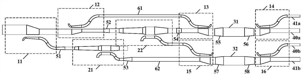
[0036] Such as figure 1 As shown, the present invention includes a transverse magnetic mode demultiplexer 11, a first transverse electric mode demultiplexer 12, a first transverse electric mode multiplexer 13, a second transverse electric mode demultiplexer 14, a second transverse electric mode Electric mode multiplexer 15, third transverse electric mode demultiplexer 16, first polarization beam splitting rotator 21, second polarization beam splitting rotator 22, first multimode nonlinear waveguide 31, second multimode nonlinear waveguide Linear waveguide 32, first single-mode output waveguide 40a, second single-mode output waveguide 40b, third single-mode output waveguide 41a, fourth single-mode output waveguide 41b, first adiabatic tapered waveguide 51, second adiabatic tapered waveguide 52. The third adiabatic tapered waveguide 53, the fourth adiaba...


PUM

PropertyMeasurementUnit
thicknessaaaaaaaaaa
thicknessaaaaaaaaaa
refractive indexaaaaaaaaaa

Abstract

The invention discloses a three-dimensional hybrid multiplexing signal all-optical wavelength conversion device on a silicon substrate. The wavelength conversion device is mainly composed of a transverse magnetic mode demultiplexer, three transverse electric mode demultiplexers, two transverse electric mode multiplexers, two polarization beam splitting rotators and two multimode nonlinear waveguides, the signal light with dual polarization, dual modes and multiple wavelengths and the pump light are input into the wavelength conversion device at the same time, and after passing through the wavelength conversion device, the signal light and the pump light are subjected to all-optical wavelength conversion to generate the idle frequency light carrying the same data as the signal light. According to the invention, multiple paths of signals can be loaded to a fundamental mode and a first high-order mode of a same multimode waveguide at the same time to form the mode multiplexing, and meanwhile, the all-optical wavelength conversion of the mixed multiplexing signals is realized by combining a polarization multiplexing technology and utilizing the dispersed and optimized multimode nonlinear waveguide, so that the transmission capacity of a communication system and the flexibility of a dynamic wavelength routing network are improved. The device can be used in the fields of wavelength routing, ultra-large capacity signal processing and the like in an all-optical communication network.

Description

technical field [0001] The invention relates to an all-optical wavelength conversion device on a silicon substrate in the field of optical waveguides, in particular to a three-dimensional hybrid multiplexing signal all-optical wavelength conversion device on a silicon substrate. Background technique [0002] All-optical wavelength switching has long been considered an ideal solution to increase the flexibility of dynamic wavelength routing networks. At the same time, with the increasing demand for high-bandwidth capacity of optical communication in today's Internet-of-everything information society, and the increasing development of planar optical waveguide integrated device technology, people began to fully tap and utilize the wavelength division multiplexing (WDM) technology in silicon-based waveguides. , mode multiplexing (MDM) technology and polarization multiplexing (PDM) technology to increase communication capacity. In order to achieve wavelength reuse in optical com...

Claims


Application Information

Patent Timeline
Patent Type & Authority Applications(China)
IPC IPC(8): G02B6/12G02B6/122G02B6/14
CPCG02B6/12004G02B6/12007G02B6/122G02B6/14G02B2006/12164G02B2006/12152
Inventor 高士明陈宝宝赵义
Owner ZHEJIANG UNIV
Why Eureka
Try Eureka