

Silicon-based three-dimensional integrated transceiving front end
A three-dimensional, silicon-based technology, applied in electrical solid devices, semiconductor devices, semiconductor/solid-state device components, etc., can solve the problems of large RF signal loss, unfavorable system integration, large volume, etc., to achieve low radiation loss, integrated The effect of high degree and small volume
Patent Information
- Authority / Receiving Office
- CN · China
- Patent Type
- Applications(China)
- Current Assignee / Owner
- Publication Date
- 2021-10-22
Smart Images
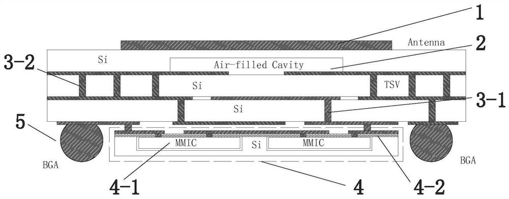
Figure 1 
Figure 2 
Figure 3
Abstract
Description
technical field
[0001] The invention relates to radio frequency communication technology, semiconductor technology and silicon-based packaging technology, in particular to a silicon-based three-dimensional integrated transceiver front end. Background technique
[0002] With the vigorous development of the 5G communication industry and radar system technology, miniaturization, light weight and low cost have become important directions for the development of the transceiver front-end. The traditional RF transceiver front-end is built with discrete components, which has the disadvantages of large volume and heavy weight, which is not conducive to system integration. At the same time, due to the interconnection mode of gold wire bonding and coaxial connectors between chips and modules, the loss of radio frequency signals is large. Three-dimensional integration technology means that the circuit is no longer limited to the X-Y plane, and high-density stacking of RF circuits can b...
Examples
Embodiment Construction
[0027] The technical solutions of the present invention will be described in detail below in conjunction with the accompanying drawings.
[0028] The present invention designs a silicon-based three-dimensional integrated transceiver front end, such as figure 1 As shown, it includes silicon-based antenna radiation layer, antenna feed network layer, radio frequency signal vertical transmission layer, packaging chip module layer and input / output port layer. The antenna feed network layer is arranged under the radiation layer of the silicon-based antenna, such as figure 2 As shown, the antenna feeding network layer includes a closed air cavity structure, the air cavity structure is processed by MEMS etching process, and the radio frequency transmission line mode in the antenna feeding network layer is a coplanar waveguide. The radio frequency signal vertical transmission layer is arranged below the antenna feed network layer, and a high-density three-dimensional vertical through...