SOC PMUT suitable for high-density system integration, array chip and manufacturing method

A technology of system integration and manufacturing method, which is applied to components of TV systems, manufacturing microstructure devices, coupling of optical waveguides, etc., can solve the problem of reducing the duty cycle, operating frequency of PMUT units, adverse effects on power consumption, and affecting PMUT arrays Uniformity and other issues, to achieve the effect of reducing chip size and system volume, high-density system integration, and realizing multi-frequency scanning in one machine

Active Publication Date: 2021-11-19
NANJING SHENGXI XINYING TECH CO LTD
View PDF9 Cites 9 Cited by
  • Summary
  • Abstract
  • Description
  • Claims
  • Application Information

AI Technical Summary

Problems solved by technology

As a result, metal routing faces two major constraints
First, if you want each cell to have its own independent top-level metal connection, as shown in Figure 2(b), you must add an additional amount of metal routing
As a result, the metal wiring reduces the duty cycle of the PMUT unit (the ratio of the area that can generate ultrasound in the unit to the entire unit area), and the metal wiring also occupies a large proportion of the chip area outside the array, and the parasitics generated by the additional metal wiring Resistors, Capacitors, have adverse effects on speed, power consumption, etc.
Second, most of today's PMUT array designs, in order to reduce additional metal wiring, share the same top-level metal connection (common column connection) with multiple cells in the same column. As a result, these cells interfere with each other (cross-talk) becomes serious, the main performance parameters of the PMUT array, such as effective frequency bandwidth, signal-to-noise ratio, etc., are adversely affected
The chip area occupied by the metal wiring is much larger than the chip area occupied by the PMUT array, which is extremely uneconomical
At the same time, the longer metal wiring length increases the parasitic effect of resistors and capacitors, which has a negative impact on the operating frequency and power consumption of the PMUT array.
The uneven length of the wiring will also directly affect the uniformity of the work of the PMUT array

Method used


Image

  • SOC PMUT suitable for high-density system integration, array chip and manufacturing method
  • SOC PMUT suitable for high-density system integration, array chip and manufacturing method
  • SOC PMUT suitable for high-density system integration, array chip and manufacturing method

Examples


Embodiment 1

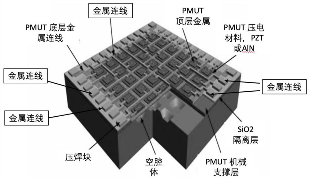
[0091] As shown in Figure 4 (a), 4 (b), this embodiment provides a kind of SOC PMUT suitable for high-density system integration, including a first wafer and a second wafer, and the first wafer arranges a silicon substrate material 160 , CMOS unit 160-CMOS with double-layer metal wiring, the second wafer arranges the mechanical layer 130, the lower metal layer 112, the piezoelectric material layer 115, the upper metal layer 114, the cavity body 120, and the CMOS auxiliary circuit of the double-layer metal wiring 300-CMOS.

[0092] The two ends of the metal interconnection layer 201 of the CMOS unit 160 -CMOS disposed above the silicon substrate 160 are vertically interconnected with two second-layer metal wirings 202 above the metal interconnection layer 201 through two metal lead holes 212 respectively. The silicon substrate 160 is provided with two silicon through-hole TSVs 162 that run through the entire silicon substrate 160, so that the two ends of the metal interconnecti...

Embodiment 2

[0103] This embodiment provides a SOC ultrasonic transducer suitable for high-density system integration, which is similar to the structure of Embodiment 1. Considering the overall design of the SOC PMUT, when the resolution requirement is high and a large-scale array is required, the interconnection Implementations may require multiple layers of wiring. For example, when artificial intelligence algorithms are also put into SOC PMUT ultrasonic design, CMOS IC design may require 5-6 layers of metal wiring. In the process flow of the present invention, the wiring structure has been specially considered, and the process flow has great flexibility in the number of wiring layers. Therefore, in this embodiment, on the basis of the first embodiment, at least one layer of metal wiring is provided above the second layer of metal wiring, and the metal wiring of each layer of the at least one layer of metal wiring is vertically interconnected through metal lead holes. , the lowermost la...

Embodiment 3

[0106] This embodiment provides a vertical electrical interconnection to replace the traditional planar wiring method to manufacture the ultrasonic transducer suitable for high-density system integration. The SOC PMUT ultrasonic transducer vertically connects the PMUT upper metal layer 114 to the stop layer metal structure 303 and the corresponding CMOS auxiliary circuit 300-CMOS second layer metal 302 respectively through the upper metal link hole ZTM163-1; The lower metal layer 112 is vertically connected to the stop layer metal structure 303 and the corresponding CMOS auxiliary circuit 300-CMOS second layer metal 302 through the lower metal link hole ZBM 163-2, and then through the two metal The lead hole 312 is vertically connected to any device in the CMOS auxiliary circuit 300-CMOS. Through reasonable wiring, series and parallel connection of multiple ultrasonic transducers can be realized.

[0107] The CMOS auxiliary circuit 300-CMOS can be connected to the CMOS unit 1...


PUM

PropertyMeasurementUnit
thicknessaaaaaaaaaa

Abstract

The invention discloses an SOC PMUT suitable for high-density system integration, an array chip and a manufacturing method. The SOC PMUT suitable for high-density system integration realizes vertical stacking and monolithic integration of an SOC PMUT array and a CMOS auxiliary circuit thereof through direct bonding of an active wafer and a multi-channel metal wire structure in the vertical direction, and extends to a packaging layer through a TSV, so that the SOC PMUT does not need to be communicated with a CMOS through pressure welding blocks on the periphery of the array, the bottleneck of traditional ultrasonic transducer metal interconnection is relieved, the chip area occupied by the ultrasonic transducer metal interconnection is greatly reduced, meanwhile, the length of metal wiring is reduced, and the bad influence of the electrical parasitic effect caused by the length on the performance of an ultrasonic transducer array is reduced.

Description

technical field [0001] The invention relates to the technical field of high-density single-chip integrated semiconductor sensors, and specifically relates to a new structure and processing technology for the integration of 3D (3dimensional) three-dimensional PMUT architecture and SOC (System-On-Chip). Background technique [0002] Ultrasonic diagnostic instrument, through its ultrasonic probe, emits ultrasonic waves to the human body, and uses various information generated by the reflection, refraction, and diffraction of sound during the propagation process of human organs and tissues to receive, amplify, and transmit information. processed to form an image or flow Doppler and finally displayed on a monitor. A medical color ultrasonic diagnostic instrument mainly includes: probe, host, control panel, display and other accessories. [0003] As human society enters the era of big medical care, the application of medical ultrasound has developed rapidly. From medical imaging...

Claims


Application Information

Patent Timeline
Patent Type & Authority Applications(China)
IPC IPC(8): B81B7/00B81B7/02B81C1/00B06B1/06
CPCB81B7/008B81B7/007B81B7/02B81C1/00238B81C1/00301B81C1/00246B06B1/06B81B2201/0271H01L24/80H01L24/94H01L23/481H01L25/0657H01L24/08H01L2224/08145H01L2224/80895H01L2224/80896H01L2224/80365H01L2225/06527H01L2225/06558H01L2225/06565H01L25/50H01L2225/06541H01L23/3171H01L21/76898A61B8/4483B06B1/0629H10N30/8554H10N30/082H10N30/076B81B2207/012B81B2207/07B81C2203/0785H01L2924/1461
Inventor 李晖尹峰
Owner NANJING SHENGXI XINYING TECH CO LTD
Why Eureka
Try Eureka