PtSx high-performance photoelectric device and preparation method and application thereof
An optoelectronic device, high-performance technology, applied in the direction of color/spectral property measurement, instrument, scientific instrument, etc., can solve the limited crystal size and price of platinum sulfide crystal, restrict the rapid progress of development and application, platinum sulfide material and device performance To achieve the effect of wide detection spectral range, large application potential and low cost
- Summary
- Abstract
- Description
- Claims
- Application Information
AI Technical Summary
Problems solved by technology
Method used
Image
Examples
Embodiment 1
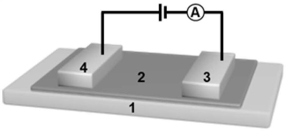
[0049] A PtS x high-performance optoelectronic devices, such as figure 1 As shown, including substrate 1, PtS grown sequentially from bottom to top x Thin layer 2, two electrodes, PtS grown on the upper surface of substrate 1 x TLC 2, PtS x The upper surface of the thin layer 2 is provided with two electrodes, 1≤x≤2.
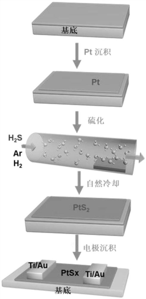
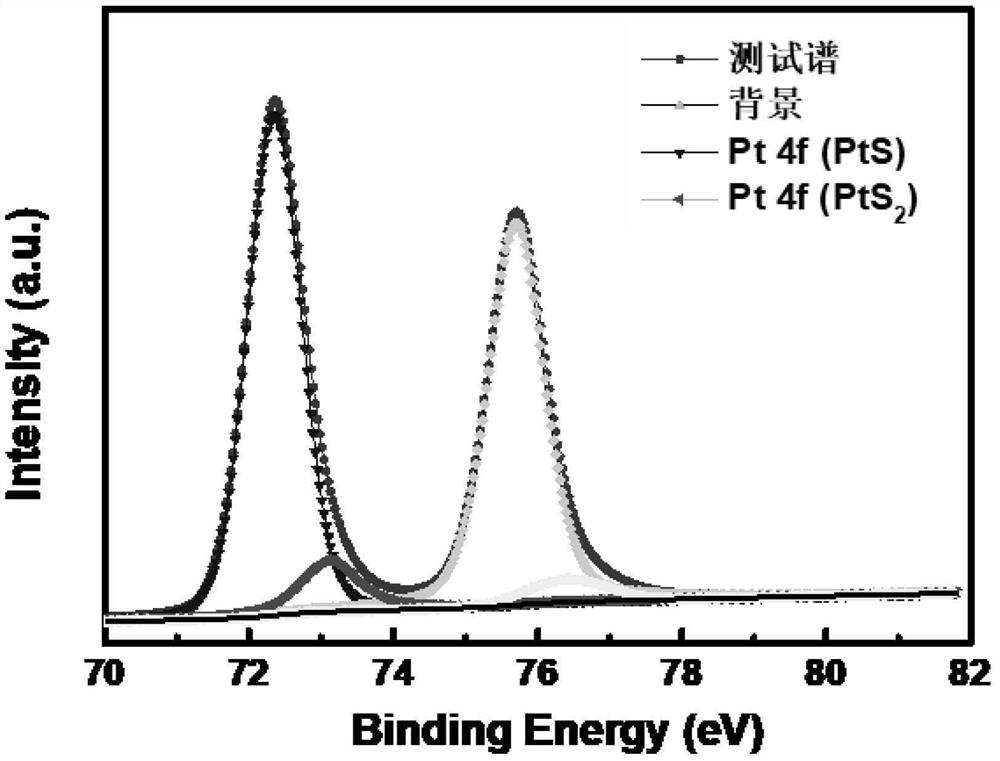
[0050] PtS x Thin layer 2 is made of PtS 2 and PtS complexes. A growth is formed.
[0051] PtS x Thin layer 2 has a thickness of 1-30 nm;
[0052]The spectral response range of the optoelectronic device is 200-1500nm.
[0053] Substrate 1 is sapphire or gallium nitride or silicon carbide.
[0054] The two electrodes include a first electrode 3 and a second electrode 4, and the first electrode 3 is any one of a Ti / Au composite electrode, a Ti / Al / Ni / Au composite electrode, and a Ti / Al / Pt / Au composite electrode, The second electrode 4 is any one of a Ti / Au combined electrode, a Ti / Al / Ni / Au combined electrode, and a Ti / Al / Pt / Au combined electrode. The ro...
Embodiment 2
[0056] According to a kind of PtS described in embodiment 1 x High-performance optoelectronic devices, the difference lies in:
[0057] PtS x Thin layer 2 has a thickness of 3-11 nm; substrate 1 is sapphire.
Embodiment 3
[0059] According to a kind of PtS described in embodiment 1 x High-performance optoelectronic devices, the difference lies in:
[0060] PtS x Thin layer 2 has a thickness of 11 nm.
[0061] PtS with a thickness of 11nm x Under the condition of thin layer 2, the optoelectronic performance of optoelectronic devices has been greatly improved, with wide spectral responsivity (ultraviolet to infrared range), low photodetection rate (9.17x10 9 Jones) and ultra-stable characteristics (only 26% reduction in photoelectric response for one year of storage in air), the performance is relatively good in platinum sulfide optoelectronic devices.
PUM
| Property | Measurement | Unit |
|---|---|---|
| thickness | aaaaa | aaaaa |
| thickness | aaaaa | aaaaa |
| thickness | aaaaa | aaaaa |
Abstract
Description
Claims
Application Information


