Method for preparing ceramic circuit board through low-temperature sintering
A ceramic circuit board, low-temperature sintering technology, used in printed circuits, printed circuit manufacturing, printed circuit secondary treatment, etc. problems, to avoid dimensional deformation, reduce sintering temperature, and save energy
- Summary
- Abstract
- Description
- Claims
- Application Information
AI Technical Summary
Problems solved by technology
Method used
Image

Examples
Embodiment 1
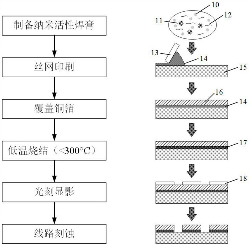
[0041] S1 selects nano-silver particles with an average particle size of 5nm, and adds 2 μm titanium particles as active metals to the silver particles, and titanium accounts for 4wt% of the total mass; add terpineol, chlorosalicylic acid and stearic acid as organic Solvent, after stirring and defoaming treatment, nano-metal active solder paste is obtained, wherein the mass of metal particles in the solder paste accounts for 65wt%;
[0042] S2 Coating an active solder paste layer on the surface of the ceramic substrate by screen printing, the thickness of the solder paste layer is 80 μm;
[0043]S3 covers the active solder paste layer with a copper foil with a thickness of 0.2mm, and sinters at a low temperature in a vacuum furnace. To remove the organic solvent in the solder paste; then raise the temperature to 230°C at a heating rate of 10°C / min, and keep it for 20 minutes; finally cool with the furnace to obtain a single-sided or double-sided ceramic copper-clad laminate; ...
Embodiment 2
[0046] S1 selects nano-copper particles with an average particle size of 10nm, and adds 1 μm of titanium, cerium, and gallium particles as active metals to the copper particles, and the active metals account for 8wt% of the total mass; add terpineol, ethyl cellulose, and chlorine Substituting salicylic acid and stearic acid as organic solvents, stirring and defoaming to obtain nano-metal active solder paste, wherein the mass of metal particles in the solder paste accounts for 75wt%;
[0047] S2 Coating an active solder paste layer on the surface of the ceramic substrate by screen printing, the thickness of the solder paste layer is 150 μm;
[0048] S3 covers the active solder paste layer with a copper foil with a thickness of 0.3mm, and sinters at a low temperature in a protective atmosphere. The temperature curve is: at a heating rate of 5°C / min, increase from room temperature to 200°C, and keep it for 20 minutes. To remove the organic solvent in the solder paste; then raise ...
Embodiment 3
[0051] S1 selects nano-copper and nano-silver mixed particles with an average particle size of 20nm, in which the ratio of copper to silver is 1:1, and 3 μm titanium and cerium particles are added to the alloy particles as active metals, and titanium and cerium account for 5wt% of the total mass Adding terpineol, ethylene glycol and ethyl cellulose as organic solvents, stirring and defoaming to obtain nano-metal active solder paste, wherein the mass of metal particles in the solder paste accounts for 70wt%;
[0052] S2 Coating an active solder paste layer on the surface of the ceramic substrate by screen printing, the thickness of the solder paste layer is 100 μm;
[0053] S3 covers the active solder paste layer with a copper foil with a thickness of 0.5mm, and performs low-temperature sintering under the condition of ultrasonic assistance. , to remove the organic solvent in the solder paste; then raise the temperature to 250°C at a heating rate of 15°C / min, and keep it warm f...
PUM
| Property | Measurement | Unit |
|---|---|---|
| diameter | aaaaa | aaaaa |
| diameter | aaaaa | aaaaa |
| thickness | aaaaa | aaaaa |
Abstract
Description
Claims
Application Information
 - R&D
- Intellectual Property
- Life Sciences
- Materials
- Tech Scout
- Unparalleled Data Quality
- Higher Quality Content
- 60% Fewer Hallucinations
Browse by: Latest US Patents, China's latest patents, Technical Efficacy Thesaurus, Application Domain, Technology Topic, Popular Technical Reports.
© 2025 PatSnap. All rights reserved.Legal|Privacy policy|Modern Slavery Act Transparency Statement|Sitemap|About US| Contact US: help@patsnap.com