Trapezoidal gallium nitride micron wire array photoelectric detector and preparation method thereof

A technology of photodetectors and micron wires, which is applied in circuits, electrical components, semiconductor devices, etc., can solve the problems of large dark current and achieve the effects of high on/off current ratio, high crystal quality, and wide detection range

Pending Publication Date: 2021-12-17
ZHEJIANG XINKE SEMICON CO LTD
View PDF6 Cites 1 Cited by
  • Summary
  • Abstract
  • Description
  • Claims
  • Application Information

AI Technical Summary

Problems solved by technology

The photoconductive detector has the advantages of simple structure, easy manufacture, and fast response, but its disadvantage is that the dark current is large

Method used


Image

  • Trapezoidal gallium nitride micron wire array photoelectric detector and preparation method thereof
  • Trapezoidal gallium nitride micron wire array photoelectric detector and preparation method thereof
  • Trapezoidal gallium nitride micron wire array photoelectric detector and preparation method thereof

Examples


Embodiment 1

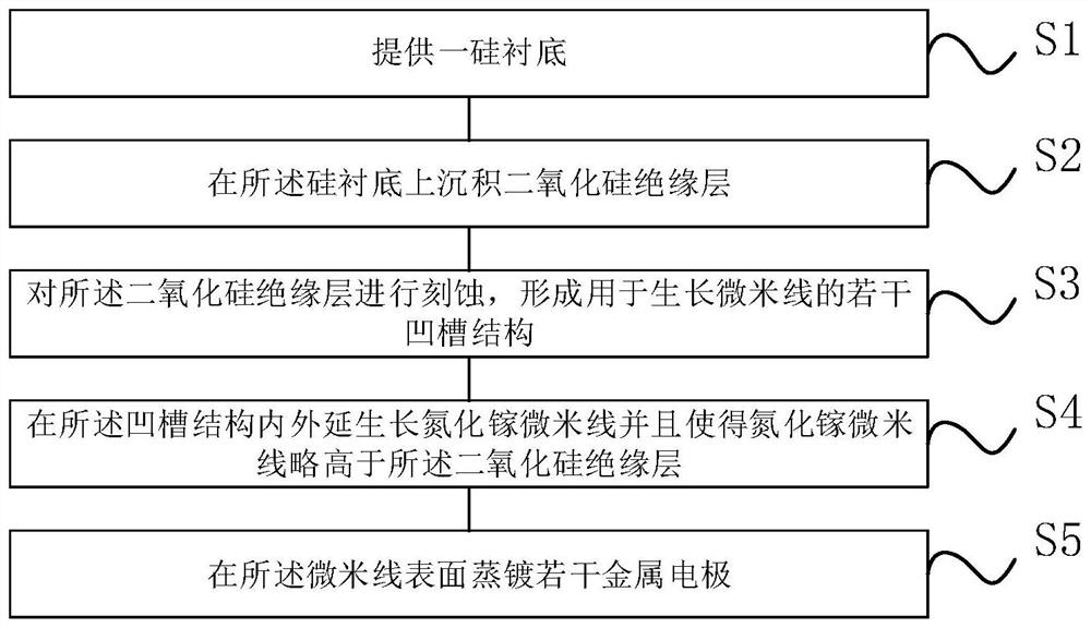
[0042] See figure 1 , figure 1 It is a schematic flow chart of a preparation method of a trapezoidal gallium nitride micro-line array photodetector provided by an embodiment of the present invention, including:

[0043] S1. Provide a silicon substrate. Specifically, the present embodiment adopts a 2-inch intrinsic type silicon wafer as a substrate, and the silicon substrate is a high-resistance silicon wafer (resistivity > 10 5 Ω·cm), the crystal orientation of the silicon wafer is .

[0044] S2. Depositing a silicon dioxide insulating layer on the silicon carbide substrate; in this embodiment, a 200nm silicon dioxide insulating layer can be formed on the surface of a 2-inch silicon wafer by thermal reduction.

[0045] S3. Etching the silicon dioxide insulating layer to form several groove structures for growing micron wires, wherein the width of the groove structure is 5-10 μm, and the depth of the groove structure is 3.5-5 μm, every two The spacing between groove structur...

Embodiment 2

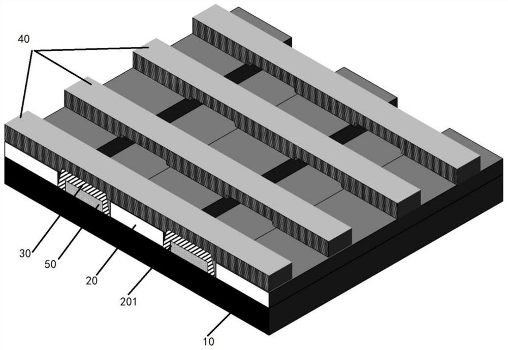
[0057] See Figure 2-Figure 7 , the trapezoidal GaN micro-line array photodetector of this embodiment can be prepared by the method of Embodiment 1, and the device includes:

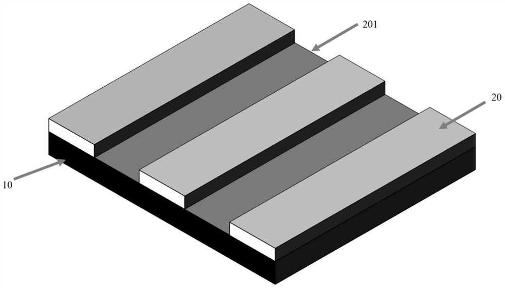
[0058] silicon substrate 10;

[0059] A silicon dioxide insulating layer 20 is formed at intervals on the silicon substrate 10, so that a plurality of groove structures 201 are formed on the substrate not covering the silicon dioxide insulating layer 20;

[0060] Gallium nitride microwires 30 are formed in the groove structure 201, and the extension direction of the gallium nitride microwires 30 is consistent with the extension direction of the groove structure 201, and the gallium nitride microwires 30 are higher than the two A silicon oxide insulating layer 20, wherein there are multiple gallium nitride micro-wires 30 in an array shape;

[0061] The aluminum nitride buffer layer 50 is formed inside the gallium nitride micro-wire 30 of the groove structure 201; the aluminum nitride buffer layer 50 can...


PUM

PropertyMeasurementUnit
widthaaaaaaaaaa
depthaaaaaaaaaa
heightaaaaaaaaaa

Abstract

The invention discloses a trapezoidal gallium nitride micron wire array photoelectric detector and a preparation method thereof. The detector comprises: a silicon substrate; silicon dioxide insulating layers formed on the silicon substrate at intervals, so that a plurality of groove structures are formed on the substrate which is not covered with the silicon dioxide insulating layers; gallium nitride micron wires formed in the groove structures, wherein the extension direction of the micron wire is consistent with the extension direction of the groove structure, and the gallium nitride micron wire is higher than the silicon dioxide insulating layer; aluminum nitride buffer layers formed in the gallium nitride micron wires of the groove structures; and a plurality of metal electrodes arranged above the gallium nitride microwires and the silicon dioxide insulating layer and perpendicular to the directions of the groove structures. According to the invention, the photoelectric detector has the good characteristics of high light/dark current, quick response, high on/off current ratio, wide detection range and the like, and the device structure is easy to grow and manufacture.

Description

technical field [0001] The invention belongs to the field of semiconductors, and in particular relates to a trapezoidal gallium nitride micro-line array photodetector and a preparation method thereof. Background technique [0002] A photodetector is a semiconductor device based on the photoelectric effect, which can absorb a certain amount of energy under light radiation to complete the conversion of an optical signal to an electrical signal. Photoelectric detectors are widely used in military, communication, medical and other fields, such as night vision, missile guidance, fire detection and other applications. [0003] Gallium nitride (GaN) is a model of the third-generation semiconductor. Because it is a group III nitride, it is insoluble in water at room temperature and resistant to strong acids and alkalis. It can only dissolve in alkalis with high temperatures at a slow rate. In an alkaline solution, the stable physical and chemical properties of gallium nitride mater...

Claims


Application Information

Patent Timeline
Patent Type & Authority Applications(China)
IPC IPC(8): H01L31/0352H01L31/0304H01L31/0224H01L31/102H01L31/18
CPCH01L31/0352H01L31/03044H01L31/022408H01L31/102H01L31/1856Y02P70/50
Inventor 李京波孙一鸣王小周
Owner ZHEJIANG XINKE SEMICON CO LTD
Why Eureka
Try Eureka