A method of producing silicon carbide seed crystals by liquid phase epitaxy

A technology of liquid phase epitaxy and silicon carbide seeds, which is applied in the direction of liquid phase epitaxy layer growth, chemical instruments and methods, single crystal growth, etc., can solve problems such as unsatisfactory transportation effect, reduce carbon solubility, and fill crystal joints, and achieve Avoid polycrystalline nucleation, graphite surface improvement, low production cost effects

Active Publication Date: 2022-02-11
CEC COMPOUND SEMICON CO LTD
View PDF14 Cites 0 Cited by
  • Summary
  • Abstract
  • Description
  • Claims
  • Application Information

AI Technical Summary

Problems solved by technology

There are many optimization schemes for liquid phase epitaxial growth, such as the schemes provided in patents CN106012021B and CN108977885A, but the fundamental problem of liquid phase growth is that the solubility of carbon in the melt is very low and the transport effect is not ideal. Patent CN110747504B provides a The growth method of silicon carbide single crystal uses rare earth and stirring to increase the solubility of graphite, but silicon carbide forms silicon carbide on the surface of graphite crucible, which further reduces the solubility of carbon, and does not solve the problem of crystal joint filling

Method used


Image

  • A method of producing silicon carbide seed crystals by liquid phase epitaxy
  • A method of producing silicon carbide seed crystals by liquid phase epitaxy
  • A method of producing silicon carbide seed crystals by liquid phase epitaxy

Examples


Embodiment 1

[0079] This embodiment provides a method for producing silicon carbide seed crystals by liquid phase epitaxy, comprising the following steps:

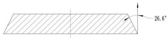
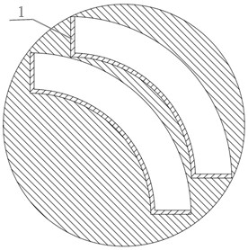
[0080] S1. Take a single crystal silicon carbide crystal with a thickness greater than 15 mm and a single crystal form of 4H, cut it into three sub-crystal plates with a thickness of 5 mm, and grind and polish the carbon and silicon surfaces of each sub-crystal plate to ensure consistency surface type, so that the surface type of the sub-crystal plate is BOW=15μm, Warp=50μm, TTV=25μm; wherein, the diameter of the single crystal region of each sub-crystal plate is not less than 150mm, refer to figure 1 As shown, the epitaxial edge of one of the sub-crystal plates is cut at 26.6° from the C-plane, and the other two sub-crystal plates, see figure 2 Shown are fan ring plates, the edge area 1 of the two fan ring plates is cut at 26.6° along the C plane, and the defect area is removed;

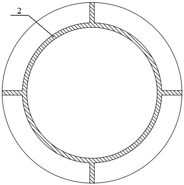
[0081] S2. Splice the sub-crystal plates according t...


PUM

PropertyMeasurementUnit
thicknessaaaaaaaaaa
thicknessaaaaaaaaaa
widthaaaaaaaaaa

Abstract

The present invention provides a method for producing silicon carbide seed crystals by liquid phase epitaxy, comprising the following steps: S1. Cutting a single crystal silicon carbide crystal of a certain thickness into a plurality of sub-crystal plates, and cutting the plurality of sub-crystal plates along the edges with C The surface is beveled at a fixed angle, and the carbon and silicon surfaces of the plurality of sub-crystal plates are ground and polished to ensure a consistent surface shape; S2, the sub-crystal plates are spliced ​​according to the target shape to obtain a splicing plate with a splicing gap, A first metal film is prepared on the silicon surface of the splice plate; S3, isostatically bonding the splice plate and the seed crystal tray to obtain a bonded crystal plate; S4, performing liquid phase epitaxy repair on the bonded crystal plate; S5, slicing processing to obtain a silicon carbide seed crystal. The method of the present invention obtains the daughter crystal plate by cutting the single crystal silicon carbide crystal, and after splicing and liquid phase epitaxy repair, it is cut into a plurality of wafers. Large-size SiC seed crystals with lower cost.

Description

technical field [0001] The invention belongs to the technical field of silicon carbide crystal growth, in particular to a method for producing silicon carbide seed crystals by liquid phase epitaxy. Background technique [0002] The third-generation semiconductor materials have gradually become the core support of the new generation of information technology. The mainstream products in the domestic silicon carbide single crystal substrate market have gradually shifted from 4-inch substrates to 6-inch substrates, and some companies in the world have 8-inch carbonized substrates. Mass production of silicon is on the agenda. At present, most domestic enterprises cannot obtain high-quality single wafers with a diameter of more than 200mm. As a seed crystal, it seriously affects the overall development progress of large-sized crystals. [0003] In order to solve this kind of situation, the current mainstream solution is to obtain large-size crystals. One is to use 4-inch or 6-inc...

Claims


Application Information

Patent Timeline
Patent Type & Authority Patents(China)
IPC IPC(8): C30B29/36C30B19/12
CPCC30B29/36C30B19/12
Inventor 潘尧波薛卫明马远
Owner CEC COMPOUND SEMICON CO LTD
Why Eureka
Try Eureka