Silicon carbide-based AlScN template for high-frequency high-performance SAW device and preparation method of silicon carbide-based AlScN template
A silicon carbide-based, high-performance technology, used in semiconductor/solid-state device manufacturing, electrical components, circuits, etc., to solve problems such as large surface roughness, abnormal nucleation, and low temperature stability
- Summary
- Abstract
- Description
- Claims
- Application Information
AI Technical Summary
Problems solved by technology
Method used
Image
Examples
Embodiment 1
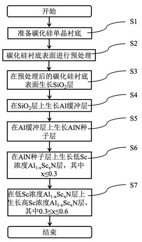
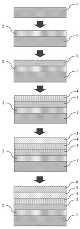
[0028] A silicon carbide-based AlScN template structure and preparation method for high-frequency high-performance SAW devices, mainly including: preparation of silicon carbide substrate 1 (S1), substrate surface pretreatment (S2), growth of SiO 2 Layer 2 (S3), growing Al layer 3 (S4), growing AlN seed layer 4 (S5), growing Al 1-x sc x N low Sc concentration layer 5 (S6), Al growth 1-x sc x N high Sc concentration layer 6 (S7). like figure 1 , 2 As shown, they are a schematic diagram of the preparation process of the silicon carbide-based AlScN template and a schematic diagram of the preparation process of the silicon carbide-based AlScN template in this embodiment, respectively. Next, the structure and preparation method of the silicon carbide-based AlScN template of this embodiment will be described in detail with reference to the accompanying drawings.
[0029]1) Prepare SiC substrate 1 (S1). Silicon carbide substrate 1 has a crystal orientation of (0001), a crystal ...
Embodiment 2
[0037] still, such as figure 1 , 2 , the structure and preparation method of the silicon carbide-based AlScN template of this embodiment will be described in detail with reference to the accompanying drawings.
[0038] 1) Prepare SiC substrate material 1 (S1). The silicon carbide substrate 1 is a polished substrate of standard specifications. The surface is an RCA-cleaned EPI-ready polished surface with a roughness of less than 0.3 nm, and the back surface is a grinding grade with a roughness of 1±0.2 μm.
[0039] 2) The surface of the substrate 1 is pretreated (S2). The pretreatment conditions are as follows: the radio frequency power is 20W, the argon gas flow range is 300sccm, and the duration is 60s. The use of pretreatment technology can remove oxide impurities on the surface of the substrate material, accumulate bombardment energy, and enhance the activity and migration ability of adatoms.
[0040] 3) Growth of SiO 2 Layer 2 (S3). Preparation of 100nm SiO 2 layer,...
PUM
| Property | Measurement | Unit |
|---|---|---|
| thickness | aaaaa | aaaaa |
| thickness | aaaaa | aaaaa |
| thickness | aaaaa | aaaaa |
Abstract
Description
Claims
Application Information


