Automatic surface mounting device based on integrated circuit design

A patch device and integrated circuit technology, applied in the direction of cleaning methods using gas flow, electrical components, electrical components, etc., can solve the problems of reduced production efficiency, low intelligence, and harmfulness

Inactive Publication Date: 2022-01-28
炬为微电子(上海)有限公司
View PDF6 Cites 1 Cited by
  • Summary
  • Abstract
  • Description
  • Claims
  • Application Information

AI Technical Summary

Problems solved by technology

[0002] Integrated circuit design can also be called ultra-large-scale integrated circuit design, which refers to the design process aimed at integrated circuits and ultra-large-scale integrated circuits. Integrated circuit design involves the establishment of electronic devices and interconnection models between devices. All devices Both components and interconnection lines need to be placed on a semiconductor substrate material. These components are placed on a single silicon substrate through the semiconductor device manufacturing process to form a circuit. The most commonly used substrate material for integrated circuit design is silicon. Design Personnel will use technical means to electrically isolate the various devices on the silicon substrate from each other to control the conductivity between the various devices on the entire chip. PN junctions, metal oxide semiconductor field effect transistors, etc. constitute the basic structure of integrated circuit devices. , and the complementary metal oxide semiconductor composed of the latter has become the basic structure of logic gates in digital integrated circuits due to its advantages of low static power consumption and high integration. Designers need to consider the energy dissipation of transistors and interconnection lines , this is different from the previous construction of circuits from discrete electronic devices, because all the devices of an integrated circuit are integrated on a silicon chip, and the electromigration of metal interconnections and electrostatic discharge are usually harmful to devices on microchips, so It is also a topic that needs to be paid attention to in the design of integrated circuits. Circuit boards are an important part of smart devices. During the production and processing of circuit boards, it is often necessary to attach some electrical components to circuit boards. The degree of automation is low, and most of them are placed manually, resulting in a greatly reduced production efficiency. At the same time, the circuit board may be damaged due to dust on the circuit board during placement.

Method used


Image

  • Automatic surface mounting device based on integrated circuit design
  • Automatic surface mounting device based on integrated circuit design
  • Automatic surface mounting device based on integrated circuit design

Examples


Embodiment Construction

[0024] The present invention will be further described below in conjunction with the accompanying drawings and embodiments.

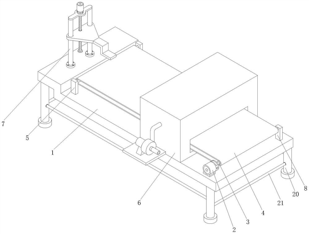
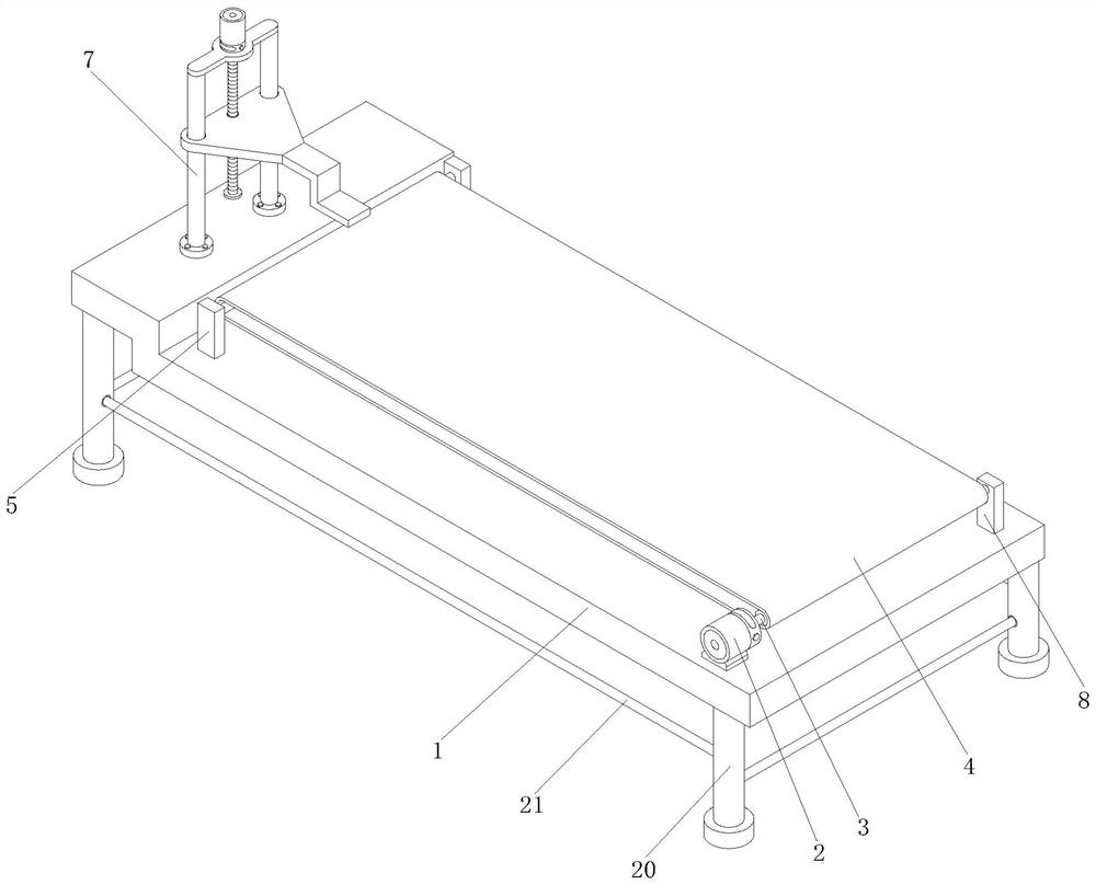
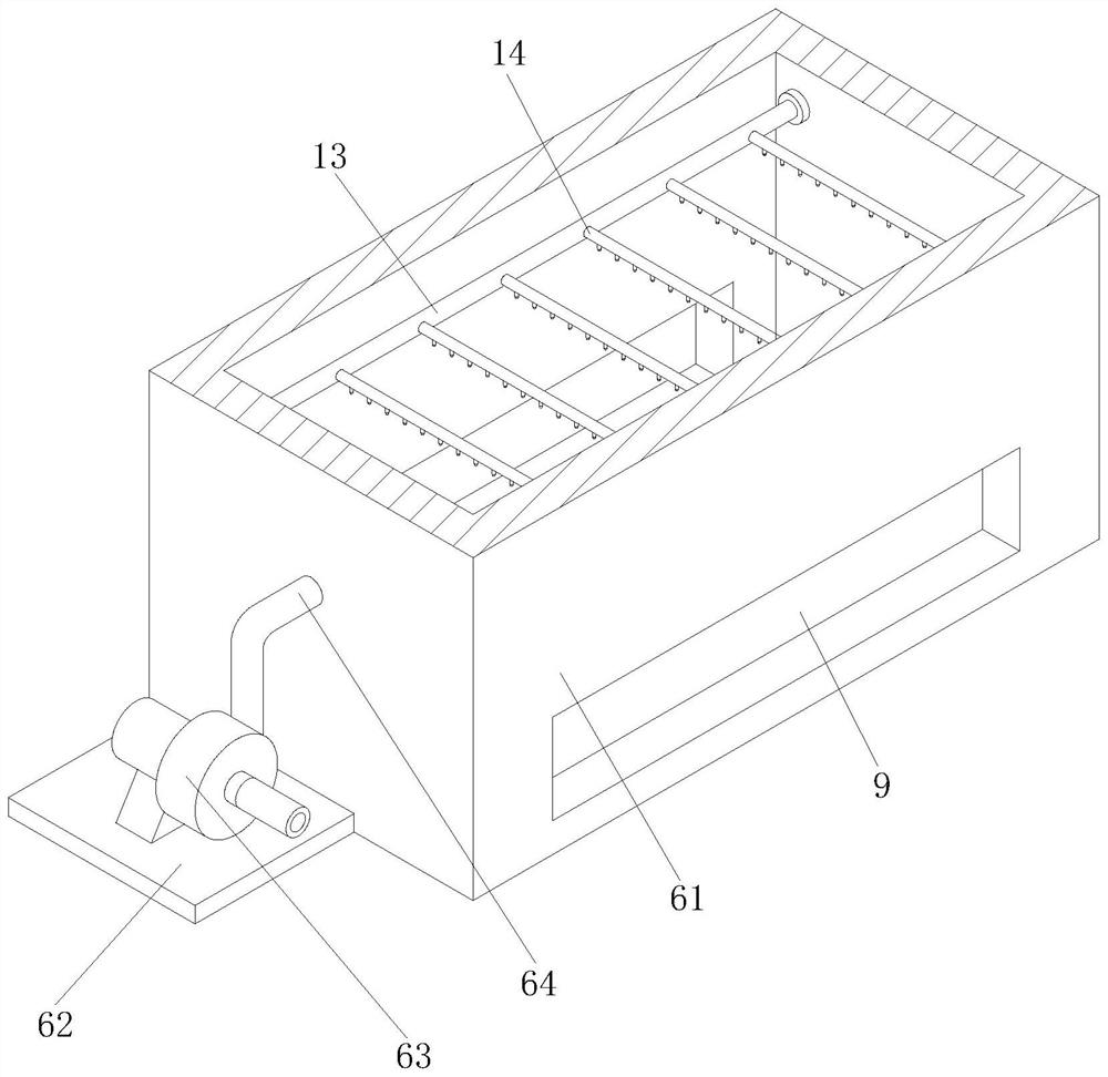
[0025] Please refer to figure 1 , figure 2 , image 3 , Figure 4 with Figure 5 ,in figure 1 A structural schematic diagram of a preferred embodiment of an automatic placement device based on integrated circuit design provided by the present invention; figure 2 for figure 1 Schematic diagram of the structure of the conveyor belt shown; image 3 for figure 1 Schematic diagram of the structure of the dust removal assembly shown; Figure 4 for figure 1 The schematic diagram of the connecting pipe and the air nozzle shown; Figure 5 for figure 1 Schematic diagram of the structure of the patch assembly shown. The automatic placement device for integrated circuit design includes workbench 1:

[0026] In the specific implementation process, such as figure 1 , figure 2 , image 3 , Figure 4 with Figure 5 As shown, the top of the workbenc...


PUM


Abstract

The invention provides an automatic surface mounting device based on integrated circuit design. The device comprises a workbench, the top of the workbench is fixedly connected with a first motor, the output end of the first motor is fixedly connected with a rotating rod, the outer side of the rotating rod is in transmission connection with a conveying belt, the inner wall of one end of the conveying belt is rotationally connected with a first fixing block through a rotating shaft, a dust removal assembly is arranged above the conveying belt, a surface mounting assembly is arranged at the top, away from the first motor, of the workbench, a dust removal box is fixedly connected to the top of the workbench and located on the outer side of the conveying belt, and one side of the dust removal box is fixedly connected with a supporting plate, and the top of the supporting plate is fixedly connected with a suction fan. The automatic surface mounting device based on the integrated circuit design has the advantages of being simple in design, convenient to use, capable of improving the working efficiency and capable of removing dust on an integrated circuit board.

Description

technical field [0001] The invention relates to the technical field of integrated circuit design, in particular to an automatic placement device based on integrated circuit design. Background technique [0002] Integrated circuit design can also be called ultra-large-scale integrated circuit design, which refers to the design process aimed at integrated circuits and ultra-large-scale integrated circuits. Integrated circuit design involves the establishment of electronic devices and interconnection models between devices. All devices Both components and interconnection lines need to be placed on a semiconductor substrate material. These components are placed on a single silicon substrate through the semiconductor device manufacturing process to form a circuit. The most commonly used substrate material for integrated circuit design is silicon. Design Personnel will use technical means to electrically isolate the various devices on the silicon substrate from each other to contr...

Claims


Application Information

Patent Timeline
Patent Type & Authority Applications(China)
IPC IPC(8): B08B5/02B08B15/00H05K13/04
CPCB08B5/023B08B15/007H05K13/046
Inventor 陈小凤
Owner 炬为微电子(上海)有限公司
Why Eureka
Try Eureka