
Vertical cavity surface emitting laser and manufacturing method thereof

A vertical cavity surface emission and laser technology, applied in lasers, laser parts, semiconductor lasers, etc., can solve the problems of restricting large-scale applications and immature processes, avoiding oxidation and multiple epitaxy processes, and reducing the difficulty of epitaxial growth. , avoid difficult effects

Pending Publication Date: 2022-02-01
苏州镓港半导体有限公司
View PDF4 Cites 0 Cited by
  • Summary
  • Abstract
  • Description
  • Claims
  • Application Information

AI Technical Summary

Problems solved by technology

[0004] The purpose of the present invention is to provide a vertical cavity surface emitting laser and its manufacturing method, which can overcome the problems of immature technology, limited large-scale application and difficult manufacturing in the prior art

Method used


Image

  • Vertical cavity surface emitting laser and manufacturing method thereof
  • Vertical cavity surface emitting laser and manufacturing method thereof
  • Vertical cavity surface emitting laser and manufacturing method thereof

Examples


Embodiment 1

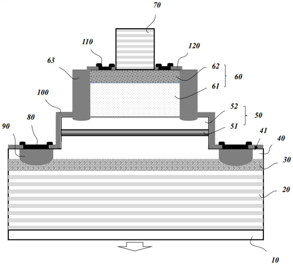
[0060] Provide a specific embodiment of a vertical cavity surface emitting laser, including a substrate 10, and a first Bragg mirror 20, a first contact layer 30, a lower cladding layer 40, an active layer 51, The upper cladding layer 52 , the current spreading layer 61 , the second contact layer 62 and the second Bragg mirror 70 .

[0061] The outer diameter of the second Bragg reflector 70 is smaller than the outer diameter of the second contact region 62, and a passivation layer 120 is arranged on the exposed surface of the second contact region 62, and a window is opened on the passivation layer 120, and a second contact region is arranged in the window. Two electrodes 110 .

[0062] The outer diameters of the current spreading layer 61 and the second contact region 62 are smaller than that of the upper cladding layer 52 and form the second mesa 60 . The side p-type diffusion of the second mesa 60 adopts Zn as a dopant, and the Zn diffusion concentration is 4E18cm -3 , a...


PUM

PropertyMeasurementUnit
widthaaaaaaaaaa
thicknessaaaaaaaaaa
diameteraaaaaaaaaa

Abstract

The invention discloses a vertical cavity surface emitting laser and a manufacturing method thereof. The laser comprises a substrate, a non-doped first Bragg reflector, a first contact layer, a non-doped lower coating layer and a non-doped first table top, and the first table top comprises an active layer and an upper coating layer which are sequentially formed on the lower coating layer; N n-type doped second table top, formed on the first table top, the second table top comprising a current expansion layer and a second contact layer which are sequentially formed on the first table top, and the side face of the second table top being subjected to p-type diffusion to form an annular diffusion region; and a non-doped second Bragg reflector formed on the second mesa. According to the invention, current limitation is carried out by using a p++ n junction depletion region through a micro-mesa side selection region p-type diffusion method, so that oxidation and multiple epitaxial processes with high difficulty and low yield are avoided. In addition, the non-doped DBR structure is adopted, so that the free carrier absorption can be reduced while the epitaxial growth difficulty is reduced.

Description

technical field [0001] The invention relates to a photoelectric device, in particular to a vertical cavity surface emitting laser and a manufacturing method thereof. Background technique [0002] Vertical Cavity Surface Emitting Laser (VCSEL) is a semiconductor laser with the advantages of small size and low threshold current. The surface emission characteristics of the laser also make it easy for fiber coupling, photon integration and on-chip testing. VCSEL has been widely used in the fields of mouse, face recognition and data center, etc. The lasing wavelength is mainly concentrated in 800-1000nm based on GaAs material system. In recent years, the rise of laser radar and gas sensing has increased the demand for VCSELs with wavelengths above 1300nm, and long-wavelength lasers are also helpful for human eye safety. The VCSEL with a wavelength of 1300-1600nm is mainly prepared by an InP-based material system. Although GaAs-based dilute nitrogen materials are also used, the m...

Claims


Application Information

Patent Timeline
Patent Type & Authority Applications(China)
IPC IPC(8): H01S5/183
CPCH01S5/18322H01S5/18347H01S5/18361
Inventor 熊敏朱杰
Owner 苏州镓港半导体有限公司
Learn More