Manufacturing method of shield gate MOSFET device with up-down structure

A manufacturing method and shielding grid technology, which are applied in semiconductor/solid-state device manufacturing, semiconductor devices, electrical components, etc., can solve the problems of large capacitance area of ​​shielding grid and control grid, reduced reliability of devices, and large input capacitance of devices, etc., to achieve Small overlap area, reduced capacitance, low cost effect

Pending Publication Date: 2022-02-11
SHANGHAI DAOZHI TECH CO LTD
View PDF0 Cites 4 Cited by
  • Summary
  • Abstract
  • Description
  • Claims
  • Application Information

AI Technical Summary

Problems solved by technology

One is to deposit polysilicon on the shielding gate and etch back into the trench to form a shielding gate, then first fill the trench above the shielding gate with HDP and etch back to a certain depth to form an inter-gate oxide layer, and then thermally oxidize the trench The gate oxide layer is formed on the sidewall. This method can accurately control the thickness of the oxide layer between the gates, but the production cost is relatively high.
The other is to deposit polysilicon on the shielding gate and etch back into the trench to form a shielding gate, then perform wet etching of the field oxide layer, and form a gate oxide layer and an inter-gate oxide layer on the trench sidewall and the top of the shielding gate at the same time through thermal oxidation , the control grid surrounds the upper part of the shielding grid like a hat, so that the capacitive area between the shielding grid and the control grid is relatively large, so the input capacitance of the device is relatively large, and there are also sharp corners at the bottom of the control grid, which is easy to make The leakage between the shield gate and the control gate becomes larger, reducing the reliability of the device

Method used


Image

  • Manufacturing method of shield gate MOSFET device with up-down structure
  • Manufacturing method of shield gate MOSFET device with up-down structure
  • Manufacturing method of shield gate MOSFET device with up-down structure

Examples


Embodiment Construction

[0037] In order to make those skilled in the art more clearly understand the purpose, technical solutions and advantages of the present invention, the present invention will be further described below in conjunction with the accompanying drawings and embodiments.

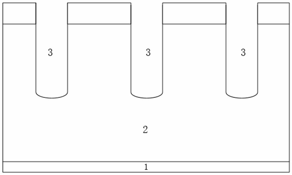
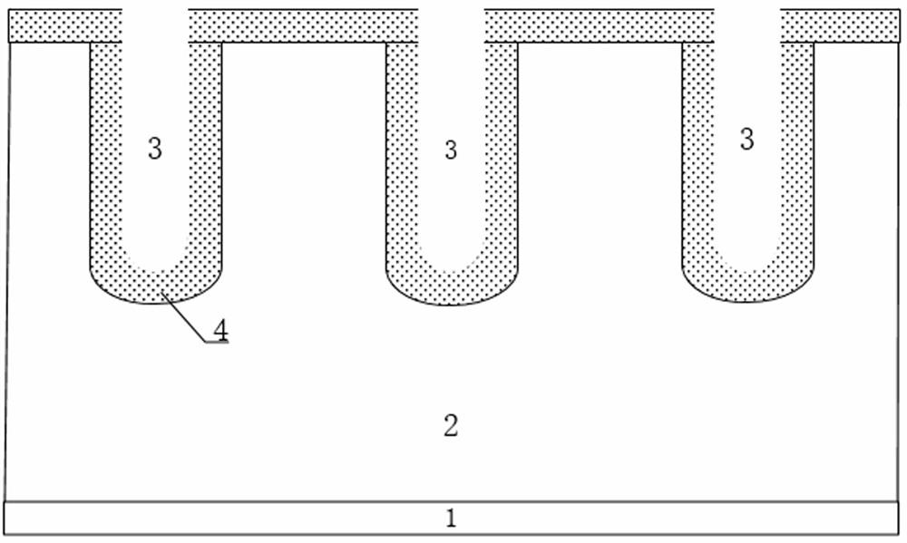
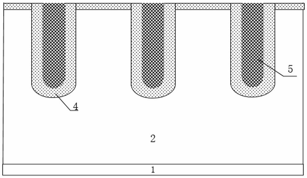
[0038] Such as Figure 1-10 As shown, the present invention proposes a method for manufacturing a shielded gate MOSFET device with a top and bottom structure, especially a relatively unique manufacturing method from the deposition of the shielded gate to the formation of the control gate. In the present invention, after the shield gate is filled and etched back to the silicon surface for the first time, a silicon nitride layer is deposited as a hard mask, and the silicon nitride layer is etched on the top of the trench in the primary cell area, and the field oxide layer is etched. , after performing the second polysilicon etching of the shielding gate, and then using a thermal oxidation process to grow an oxide laye...


PUM


Abstract

The invention discloses a manufacturing method of a shield gate MOSFET with an up-down structure. The manufacturing method comprises the following steps of: performing groove etching on a selected epitaxial silicon substrate; preparing a field oxide layer in a thermal oxidation or thermal oxidation and oxide layer deposition mode; after the shield gate polycrystalline silicon is filled, carrying out first back etching to the silicon surface; depositing a silicon nitride hard mask layer, then photoetching and etching an active region, and leaving an active region window in the silicon nitride layer; performing field oxide layer wet etching in the active region window, and carrying out second shield gate polycrystalline silicon back etching, wherein the surface of the shield gate polycrystalline silicon is 0.1 micrometer lower than the surface of the field oxide layer in the groove after the second shield gate polycrystalline silicon back etching is carried out; removing the oxide layer on the silicon surface and a part of field oxide layer in the groove by wet etching, so that the height difference between the shield gate and the field oxide layer in the groove is within 0.2 micron; simultaneously oxidizing the side walls of the groove and the shield gate to form a gate oxide layer and an inter-gate oxide layer; and filling and back-etching the gate polycrystalline silicon to form a control gate.

Description

technical field [0001] The invention relates to the technical field of design and manufacture of a shielded gate MOSFET (SGT-MOSFET) device, in particular to a method for manufacturing a shielded gate MOSFET device with an upper and lower structure. Background technique [0002] Compared with the traditional trench MOSFET, the shielded gate MOSFET device has the advantages of low on-resistance and low switching loss, so its application in the medium and low voltage power semiconductor market is gradually increasing. The gate of the shielded gate trench MOSFET structure includes both a shielded gate and a control gate. The existence of the shielded gate makes the vertical electric field similar to and rectangularly distributed when the device breaks down. Compared with the traditional trench MOSFET, the epitaxy with a smaller resistivity is easier A higher breakdown voltage can be obtained, so that the device has a smaller on-resistance. According to the relative positions o...

Claims


Application Information

Patent Timeline
Patent Type & Authority Applications(China)
IPC IPC(8): H01L21/336H01L21/28
CPCH01L29/66734H01L21/28035H01L21/28114
Inventor 陈雪萌王艳颖钱晓霞汤艺
Owner SHANGHAI DAOZHI TECH CO LTD
Why Eureka
Try Eureka