Platinum doping method of fast recovery diode

A recovery diode and platinum doping technology, which is applied in semiconductor devices, electrical components, circuits, etc., can solve the problems of low efficiency of minority carrier lifetime control and low reliability of leakage current, and achieve high softness, reduced defect concentration, and short turn-off the effect of time

Active Publication Date: 2022-02-25
YANGZHOU GUOYU ELECTRONICS
View PDF9 Cites 3 Cited by
  • Summary
  • Abstract
  • Description
  • Claims
  • Application Information

AI Technical Summary

Problems solved by technology

[0005] This application provides a platinum doping method for fast recovery diodes, which solves the low efficiency of minority carrier lifetime control and leakage current caused by the uniform doping of platinum in chips in the prior art The problem of low reliability achieves a better performance trade-off

Method used


Image

  • Platinum doping method of fast recovery diode
  • Platinum doping method of fast recovery diode
  • Platinum doping method of fast recovery diode

Examples


Embodiment

[0038] A platinum doping method for a fast recovery diode, comprising the following steps:

[0039] Material preparation: N-type silicon material is used as the substrate, and the resistivity of the material is designed according to the withstand voltage of the target product;

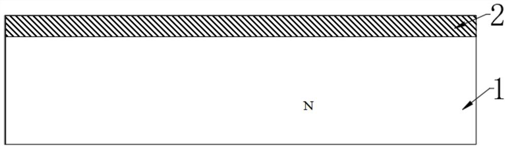
[0040] Preparation of field oxide layer: at 700°C to 1100°C, inject H2 and O2 to grow an oxide layer 2 of 1 μm to 2 μm on the front side of N-type silicon substrate 1, such as figure 1 shown;

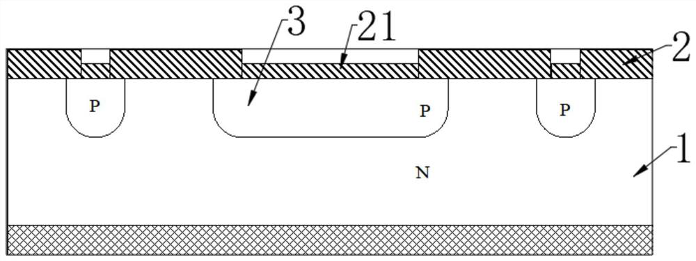
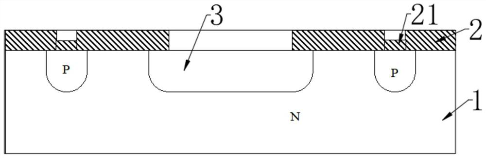
[0041] Preparation of PN junction: Open a doping window on the oxide layer 2 by photolithography and etching, and form a P-type doped region 3 by boron ion implantation, and then undergo an annealing treatment. The annealing temperature is 1100°C to 1200°C. A thin oxide layer 21 is formed on the surface of the P-type doped region, such as figure 2 As shown; the P-type doped region 3 includes a main junction and a voltage divider ring, and the voltage divider ring is located in the terminal area of ​​the chip;...


PUM

PropertyMeasurementUnit
thicknessaaaaaaaaaa
thicknessaaaaaaaaaa

Abstract

The invention discloses a platinum doping method of a fast recovery diode in the technical field of semiconductor power devices. The platinum doping method comprises the following steps: growing an oxide layer on the front surface of an N-type silicon substrate; forming a doping window on the oxide layer and injecting boron ions to form a P-type doping region, then performing annealing treatment, and forming a thin oxide layer on the surface of the P-type doping region after annealing; forming a contact hole of a front electrode on the thin oxide layer; depositing polycrystalline silicon on the front surface of the oxide layer to form a polycrystalline silicon layer, wherein the polycrystalline silicon is in contact with the P-type doped region through a contact hole; and sputtering or evaporating a platinum metal layer on the back surface of the N-type silicon substrate. The diode chip prepared by the method has shorter turn-off time, smaller reverse overshoot current and higher softness; meanwhile, the electric leakage possibility of the chip is reduced, and the reliability of the chip is improved.

Description

technical field [0001] The invention relates to the technical field of semiconductor power devices, in particular to a platinum doping method for fast recovery diodes. Background technique [0002] Fast recovery diodes are a very important switching device, and have been widely used in various electronic devices, especially switching power supplies. With the continuous improvement of the operating frequency of the device, the requirements for various indicators of the fast recovery diode are also continuously improved. [0003] The platinum doping method of the conventional fast recovery diode chip is to deposit metallic platinum on the front or back of the chip. Platinum is a fast diffusion impurity in silicon and can be quickly distributed in the entire silicon chip in the form of gaps, and then high temperature annealing is used. The method activates it into a replacement atom and forms a deep-level recombination center to control the minority carrier lifetime. [0004]...

Claims


Application Information

Patent Timeline
Patent Type & Authority Applications(China)
IPC IPC(8): H01L29/06H01L21/329H01L29/868
CPCH01L29/0603H01L29/6609H01L29/868
Inventor 李浩马文力金银萍王伟陆阳
Owner YANGZHOU GUOYU ELECTRONICS
Why Eureka
Try Eureka