Avalanche photodiode array detector

A diode array, avalanche photoelectric technology, applied in photovoltaic power generation, electric solid state devices, circuits, etc., can solve the problem of unable to suppress dark current or dark count rate of devices, and achieve the effect of reducing dark current or dark count rate

Pending Publication Date: 2022-03-04
江苏尚飞光电科技股份有限公司
View PDF0 Cites 1 Cited by
  • Summary
  • Abstract
  • Description
  • Claims
  • Application Information

AI Technical Summary

Problems solved by technology

[0003] In view of the shortcomings of the prior art described above, the object of the present invention is to provide an avalanche photodiode array detector, which is used to solve the problem that the dark current or dark count rate of the device cannot be suppressed while improving the photon detection efficiency in the prior art. question

Method used


Image

  • Avalanche photodiode array detector
  • Avalanche photodiode array detector
  • Avalanche photodiode array detector

Examples


Embodiment 1

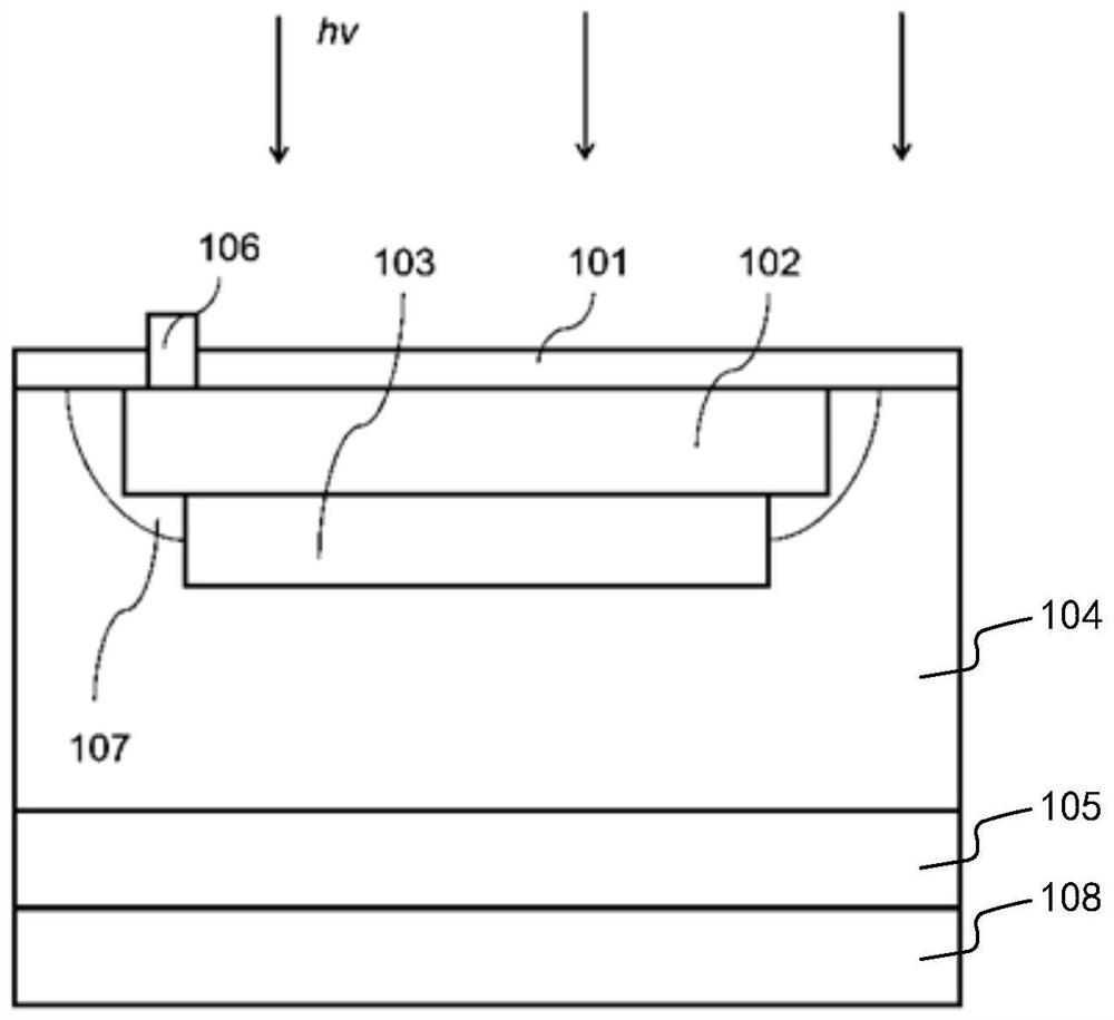
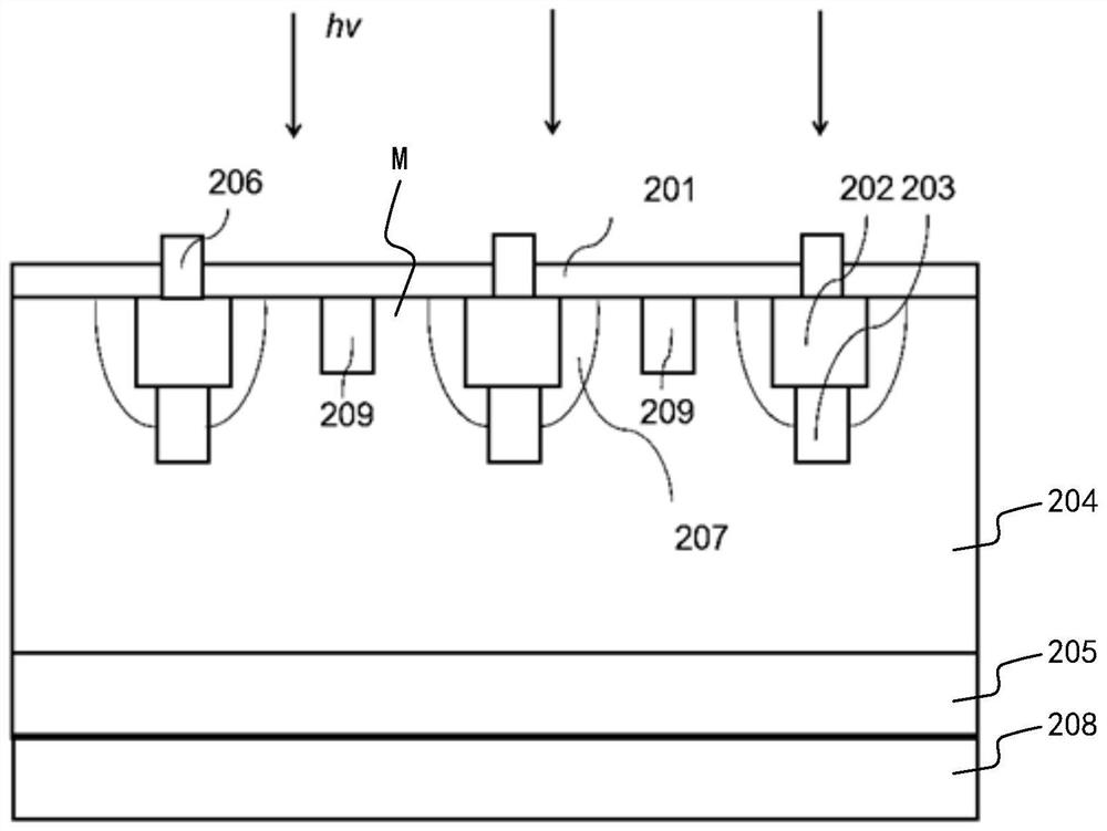
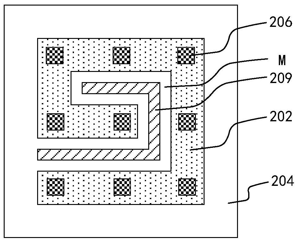
[0054] see figure 2, is a schematic cross-sectional view showing a simplified structure of a single pixel structure in the avalanche photodiode array detector of this embodiment, including a first conductivity type substrate layer 205, a first conductivity type semiconductor layer 204, a PN junction, an isolation structure 209, At least one anode terminal 206 and a cathode terminal 208, wherein the first conductivity type semiconductor layer 204 is located on the first conductivity type substrate layer 205; the PN junction is located in the first conductivity type semiconductor layer 204 And includes the doped layer 203 of the first conductivity type and the doped layer 202 of the second conductivity type arranged in sequence from bottom to top, wherein the projection of the PN junction on the horizontal plane has an interval region M; the isolation structure 209 is located at the In the semiconductor layer 204 of the first conductivity type, and located in the spacer region ...

Embodiment 2

[0071] This embodiment adopts basically the same technical solution as Embodiment 1, the difference is that in Embodiment 1, the isolation structure 209 is obtained based on the doping of the first conductivity type semiconductor layer 204, while in this embodiment, the The isolation structure 209 adopts a trench structure.

[0072] see Figure 7 , which is a schematic cross-sectional view showing a simplified structure of a single pixel structure in the avalanche photodiode array detector in this embodiment, wherein the isolation structure 209 includes a trench 209a and an isolation material filled in the trench 209a 209b, the trench 209a is opened from the top surface of the first conductivity type semiconductor layer 204 and extends downward, and the bottom surface of the trench is higher than the bottom surface of the PN junction.

[0073] As an example, the trench 209a can be obtained by wet etching the semiconductor layer 204 of the first conductivity type, and the side...

Embodiment 3

[0076] This embodiment adopts basically the same technical solution as Embodiment 1 or Embodiment 2, the difference is that in Embodiment 1 or Embodiment 2, the spacer region M does not completely separate the PN junction, and the PN junction The junction is still a whole, but in this embodiment, the spacer region M divides the PN junction into at least two independent parts located in the first conductivity type semiconductor layer 204 .

[0077] It should be pointed out that although the PN junction includes at least two independent parts located in the first conductivity type semiconductor layer 204 , these independent parts are electrically connected together through the anode terminal 106 .

[0078] In summary, in the avalanche photodiode array detector of the present invention, the projection of the PN junction of a single pixel on the horizontal plane has a spacer region, so that the partial region of the PN junction is in a separated state, and is isolated by an isolati...


PUM


Abstract

The invention provides an avalanche photodiode array detector which comprises a first conductive type substrate layer, a PN junction, an isolation structure, at least one anode leading-out end and a cathode leading-out end, a first conductive type semiconductor layer is located on the first conductive type substrate layer, the PN junction is located in the first conductive type semiconductor layer, and the isolation structure is located in the first conductive type semiconductor layer. The projections of the PN junctions on the horizontal plane are provided with interval regions; the isolation structure is located in the first conductive type semiconductor layer and located in the PN junction interval region, and the isolation structure is not in contact with the PN junction. In the invention, the projection of the PN junction of the single pixel on the horizontal plane has the interval region, so that the sum of the widths of the PN junctions of the single pixel is reduced, the whole PN junction region and the region between the PN junctions can absorb incident photons, and the reduction of the heavily doped second conductive type doping layer can improve the absorption of part of short-wavelength photons, so that the photoelectric conversion efficiency is improved. Therefore, the photon detection efficiency of the avalanche photodiode is not affected, and the dark current or dark counting rate of a single pixel is reduced.

Description

technical field [0001] The invention belongs to the field of optoelectronic technology and relates to an avalanche photodiode array detector. Background technique [0002] Single photon detectors include photomultiplier tube (Photomultiplier Tube, PMT for short), analog or digital silicon photomultiplier (Silicon Photomultiplier, SiPM for short), single photon avalanche photodiode (Single Photon Avalanche Diode, SPAD) and other types, among which, Due to the shortcomings of PMTs such as large size, high operating voltage, high power consumption, easy damage, low detection efficiency due to photocathode limitations, sensitivity to magnetic fields, and unsuitability for large-scale arrays, the application of single-photon detectors is limited. . For this reason, an analog silicon-based photomultiplier has been proposed. When designing an avalanche photodiode (APD), it is hoped to obtain a higher photon detection efficiency (PDE) and a lower photon detection efficiency. Dark ...

Claims


Application Information

Patent Timeline
Patent Type & Authority Applications(China)
IPC IPC(8): H01L31/02H01L31/0352H01L31/107H01L27/144
CPCH01L27/1443H01L27/1446H01L31/107H01L31/03529H01L31/02027Y02E10/50
Inventor 卞剑涛胡海帆盛振
Owner 江苏尚飞光电科技股份有限公司
Why Eureka
Try Eureka