Epoxy composition for packaging optoelectronic device, packaging structure and optoelectronic device

A technology for optoelectronic devices and components, which is applied in the direction of electric solid devices, electrical components, semiconductor devices, etc., can solve the problems of incapacity to encapsulate, fall off, and crack, and achieve the effect of improving heat resistance and corrosion resistance, and reducing volume shrinkage.

Pending Publication Date: 2022-03-18
XIAN SMART MATERIALS CO LTD
View PDF4 Cites 0 Cited by
  • Summary
  • Abstract
  • Description
  • Claims
  • Application Information

AI Technical Summary

Problems solved by technology

However, the above packaging structure has the problem of poor adhesion, which is easy to cause cracking, falling off, etc., and cannot be effectively packaged.

Method used


Image

  • Epoxy composition for packaging optoelectronic device, packaging structure and optoelectronic device
  • Epoxy composition for packaging optoelectronic device, packaging structure and optoelectronic device
  • Epoxy composition for packaging optoelectronic device, packaging structure and optoelectronic device

Examples


Embodiment 1

[0082] Example 1: Preparation of an epoxy composition for encapsulating optoelectronic devices

[0083] The components used are described below:

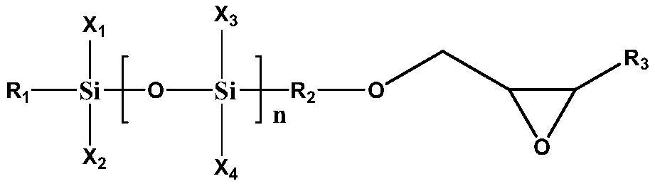
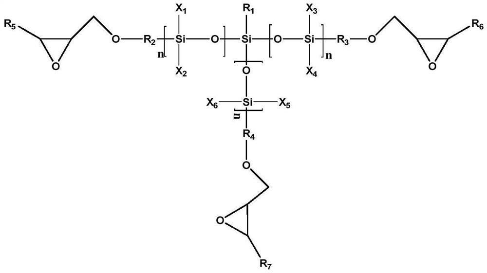
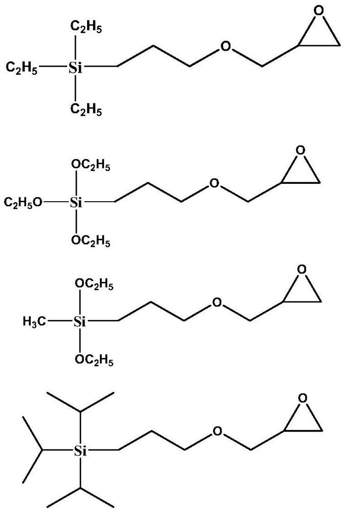
[0084] (A) silicon-containing epoxy monomer: (A1) monomer of formula 5; (A2) monomer of formula 9;

[0085] (B) Photocurable monomer: (B1) phenethyl-1,2-epoxypropyl ether, (B2) 2-hydroxy-di(1,2-epoxy) propyl ethyl propanol;

[0086] (C) Initiator: triarylsulfonium salt.

[0087] In a brown glass bottle, add 10% (A1), 40% (B1), 45% (B2) and 5% (C) of the total mass, shake and mix at room temperature for 2 hours, and then filter to obtain the composition for packaging 1; Then apply the composition on the surface of the ITO substrate by inkjet printing to form a sample with an area size of 10cm×10cm×10μm (length×width×thickness), and then pass 100mW / cm 2 The UV curing equipment cures the packaging composition by ultraviolet curing for 10 to 30 seconds, and finally forms a packaging protective film.

[0088] The performance evaluati...

Embodiment 2

[0094] Example 2: Preparation of an epoxy composition for encapsulating optoelectronic devices

[0095] A detailed description of the components used follows:

[0096] (A) silicon-containing epoxy monomer: (A1) monomer of formula 5; (A2) monomer of formula 9;

[0097] (B) Photocurable monomer: (B1) phenethyl-1,2-epoxypropyl ether, (B2) 2-hydroxy-di(1,2-epoxy) propyl ethyl propanol;

[0098] (C) Initiator: triarylsulfonium salt.

[0099]In a brown glass bottle, add 10% (A2), 40% (B1), 20% (B2) and 5% (C) of the total mass, shake and mix at room temperature for 2 hours, then filter to obtain the composition for packaging 2; Then apply the composition on the surface of the ITO substrate by inkjet printing to form a sample with an area size of 10cm×10cm×10μm (length×width×thickness), and then pass 100mW / cm 2 The UV curing equipment cures the packaging composition by ultraviolet curing for 10 to 30 seconds, and finally forms a packaging protective film.

Embodiment 3

[0100] Example 3: Preparation of an epoxy composition for encapsulating optoelectronic devices

[0101] The components used are described in detail as follows:

[0102] (A) silicon-containing epoxy monomer: (A1) monomer of formula 5; (A2) monomer of formula 9;

[0103] (B) Photocurable monomer: (B1) phenethyl-1,2-epoxypropyl ether, (B2) 2-hydroxy-di(1,2-epoxy) propyl ethyl propanol;

[0104] (C) Initiator: triarylsulfonium salt.

[0105] In a brown glass bottle, add 70% (A1), 5% (B1), 25% (B2) and 5% (C) of the total mass, shake and mix at room temperature for 2 hours, and then filter to obtain the composition for packaging 3; Then apply the composition on the surface of the ITO substrate by inkjet printing to form a sample with an area size of 10cm × 10cm × 10μm (length × width × thickness), and then pass 100mW / cm 2 The UV curing equipment cures the packaging composition by ultraviolet curing for 10 to 30 seconds, and finally forms a packaging protective film.


PUM

PropertyMeasurementUnit
transmittivityaaaaaaaaaa

Abstract

The invention discloses an epoxy composition for packaging a photoelectronic device, a packaging structure and the photoelectronic device. The epoxy composition comprises 10-70% of a photocurable monomer; 10%-70% of a single or three-functionality silicon-containing epoxy monomer; by using the silicon-containing epoxy monomer, on one hand, the silicon-containing epoxy monomer can play a role in dispersing stress, reducing internal stress and improving the mechanical property of the organic packaging composition when being impacted by force due to the fact that the deformability of a Si-O-Si chain segment of the silicon-containing epoxy monomer is high; on the other hand, the adhesive force of the organic packaging composition can be effectively improved, and the service life of a device can be effectively prolonged when the organic packaging composition is used for film packaging of an optoelectronic device.

Description

technical field [0001] The invention belongs to the technical field of organic thin films, and relates to an epoxy composition for packaging optoelectronic devices, a packaging structure and optoelectronic devices. Background technique [0002] Organic light-emitting diodes (OLEDs) are self-luminous devices that emit light by electrically exciting organic light-emitting materials, and are widely used in various fields because of their high efficiency and environmental protection. And the display unit of the organic light emitting display device may be deteriorated due to permeation of oxygen or water. Therefore, in order to achieve the purpose of prolonging the service life of the device, it is very important to effectively package the device and isolate the functional layer of the device from moisture, oxygen, etc. in the surrounding environment. At present, in the thin film encapsulation technology, a common method is to alternately laminate organic encapsulation layers a...

Claims


Application Information

Patent Timeline
Patent Type & Authority Applications(China)
IPC IPC(8): C08G59/22C08G59/32C08G59/68H01L51/52
CPCC08G59/223C08G59/3281C08G59/68H10K50/844
Inventor 吴朝新何鑫张凯
Owner XIAN SMART MATERIALS CO LTD
Why Eureka
Try Eureka