Flexible grating film and preparation method and application thereof
A grating and thin film technology, applied in the field of grating production, can solve the problems of easy damage, thickness and precision can not be guaranteed, and achieve the effect of smooth surface, regular shape error, low cost production
- Summary
- Abstract
- Description
- Claims
- Application Information
AI Technical Summary
Problems solved by technology
Method used
Image
Examples
preparation example Construction
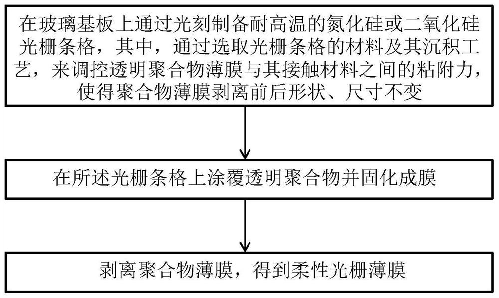
[0033] The present invention improves the preparation process of the existing flexible grating film, and prepares the flexible grating film by stripping the grid substrate layer, so as to achieve the invention goals of regulating the stripping effect of the flexible grating film, adapting to lenses of different sizes and curvatures, and simplifying the processing technology. The general implementation method is to make a photoresist grid on a glass substrate by photolithography, deposit silicon nitride in the photoresist grid to form a silicon nitride grid substrate, and coat the silicon nitride grid substrate The coated polymer is cured to form a film, and the flexible grating film is prepared after peeling off.
[0034] Factors affecting the preparation of PI grating films mainly involve several factors such as master material, master surface characterization, process method, and process parameters. In order to make the material of the grating master plate obtain satisfactor...
Embodiment 1
[0047] A preparation method for a flexible grating film, specifically comprising the steps of:
[0048] In the first step, the glass substrate is ultrasonically cleaned and dried with deionized water and isopropanol;
[0049] In the second step, the photoresist is evenly spin-coated on the glass substrate, and the rotation speed is 1000r-3s, 4000r-35s;
[0050] The third step is to use a photolithography machine to expose the grating pattern mask on the photoresist twice, and the time is 1.5s and 20s;
[0051] The fourth step is to soak the photoresist plate in the developer solution for 50s, and form a grid pattern structure after development;
[0052] In the fifth step, use PECVD at 100°C to deposit silicon nitride material on the substrate layer of the grid pattern structure for 10 minutes and 48 seconds;
[0053] The sixth step is to use acetone, DMAC, and DMF to remove the remaining photoresist to form a silicon nitride grid pattern substrate layer;
[0054] The sevent...
PUM
| Property | Measurement | Unit |
|---|---|---|
| thickness | aaaaa | aaaaa |
Abstract
Description
Claims
Application Information


