
Eureka
For R&D, Eureka makes reading and utilizing patents & technical documents easy.
Eureka AIR
Designed for self-driven R&D workflows. Generate viable solutions, solve complex R&D challenges, empower your innovation with AI.

Eureka Materials
Designed for material experts only. Revolutionize your material R&D, from search, analyze, to developing new materials.

TechResearch
Generate reliable direction feasibility study reports for your R&D in just a few steps.

TechSeek
Discover and master advanced knowledge NOW. Basics, ideas, possibilities, all at once.

TechMind
As an expert in R&D Theories, TechMind can generates customized viable solutions instantly.

TechRisk
Analyze your overall solution with one click, know your potential R&D risks in advance.

TechMonitor
Get weekly tech updates, stay abreast of the latest tech innovations and key insights.
Photoelectric detector based on TaIrTe4/Si heterojunction and preparation method thereof
A photodetector and heterojunction technology, applied in circuits, electrical components, semiconductor devices, etc., can solve the problems of low detection rate, low responsivity, narrow detection wavelength range, etc., and achieve stable and reproducible optical switching curves. Good, easy-to-operate effect
- Summary
- Abstract
- Description
- Claims
- Application Information
AI Technical Summary
Problems solved by technology
Method used
Image

Examples
Embodiment 1
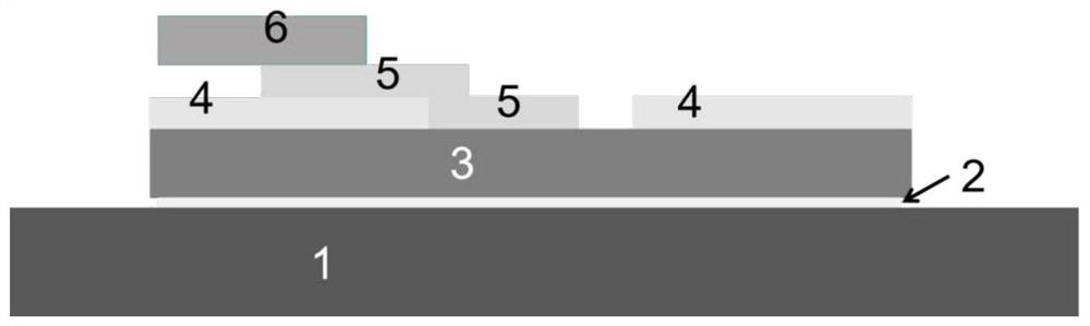
[0031] figure 1 For the present invention based on TaIrTe 4 / Si heterojunction photodetector structure schematic diagram, such as figure 1 shown. Among them, metal plate bottom electrode 1, silver paste 2, three-dimensional Si 3, silicon dioxide layer 4, TaIrTe 4 Layer 5, top electrode 6. The photodetector is based on TaIrTe 4 / Si heterojunction photodetector with a top electrode structure of 6 / TaIrTe 4 / Si heterojunction 5 / bottom electrode 1, the TaIrTe 4 / Si heterojunction is in Si / SiO 2 The Si window is etched on the substrate to make the TaIrTe 4 Nanosheets are obtained in full contact with Si, and in TaIrTe 4 TaIrTe outside the Si heterojunction 4 The edge makes the top electrode.
[0032] In this embodiment, the bottom metal plate electrode is a copper plate, and the Si substrate and the copper plate are pasted together with silver paste, and dried on a hot table, so as to ensure ohmic contact between the copper plate and the Si substrate; in addition, the th...
Embodiment 2
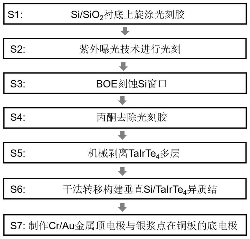
[0034] A TaIrTe-based 4 / Si heterojunction photodetector preparation method, such as figure 2 shown, including the following steps:
[0035] 1. On Si / SiO2 2 Spin-coat photoresist on the substrate at a speed of 4000 rpm, and dry on a hot stage at 100°C for 4 minutes;
[0036] 2. Using ultraviolet lithography technology, the Si / SiO coated with photoresist 2 The area of the substrate is photoetched out to 500×500μm 2 window, and developed, blow dry with nitrogen gun;
[0037] 3. Soak the substrate with a window in buffered oxide etchant (BOE) for about 1 min, then take it out, wash it with clean water 3-4 times, and blow it dry with a nitrogen gun;
[0038] 4. Soak the film processed in step 3 in acetone solution for about 10s, wash off the photoresist, rinse with water 1-2 times, dry it with a nitrogen gun, and dry it in Si / SiO 2 The middle area of the substrate gets 500 x 500 μm 2 Dimensions of the Si window;
[0039] 5. Repeatedly overlap with thermal release tape...
PUM
| Property | Measurement | Unit |
|---|---|---|
| thickness | aaaaa | aaaaa |
| thickness | aaaaa | aaaaa |
| thickness | aaaaa | aaaaa |
Abstract
Description
Claims
Application Information
 - R&D Engineer
- R&D Manager
- IP Professional
- Industry Leading Data Capabilities
- Powerful AI technology
- Patent DNA Extraction
Browse by: Latest US Patents, China's latest patents, Technical Efficacy Thesaurus, Application Domain, Technology Topic, Popular Technical Reports.
© 2024 PatSnap. All rights reserved.Legal|Privacy policy|Modern Slavery Act Transparency Statement|Sitemap|About US| Contact US: help@patsnap.com