White light LED chip and device packaged by inorganic material, and preparation method and application of white light LED chip and device
A technology of LED chips and inorganic materials, applied in the direction of electric solid devices, semiconductor devices, electrical components, etc., can solve the problems of many chip defects and cannot be used in practice, achieve small light decay, good thermal stability, and improve the consistency of light color. sexual effect
- Summary
- Abstract
- Description
- Claims
- Application Information
AI Technical Summary
Problems solved by technology
Method used
Image

Examples
Embodiment 1
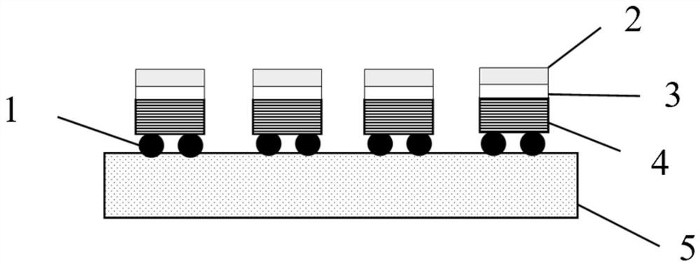
[0094] Step 1: growing an epitaxial structure based on a sapphire (alumina) single crystal substrate, including an N-type epitaxial layer, a light-emitting layer, and a P-type epitaxial layer.
[0095] Step 2: Fabricate a flip-chip wafer containing multiple LED chips on the epitaxial structure.
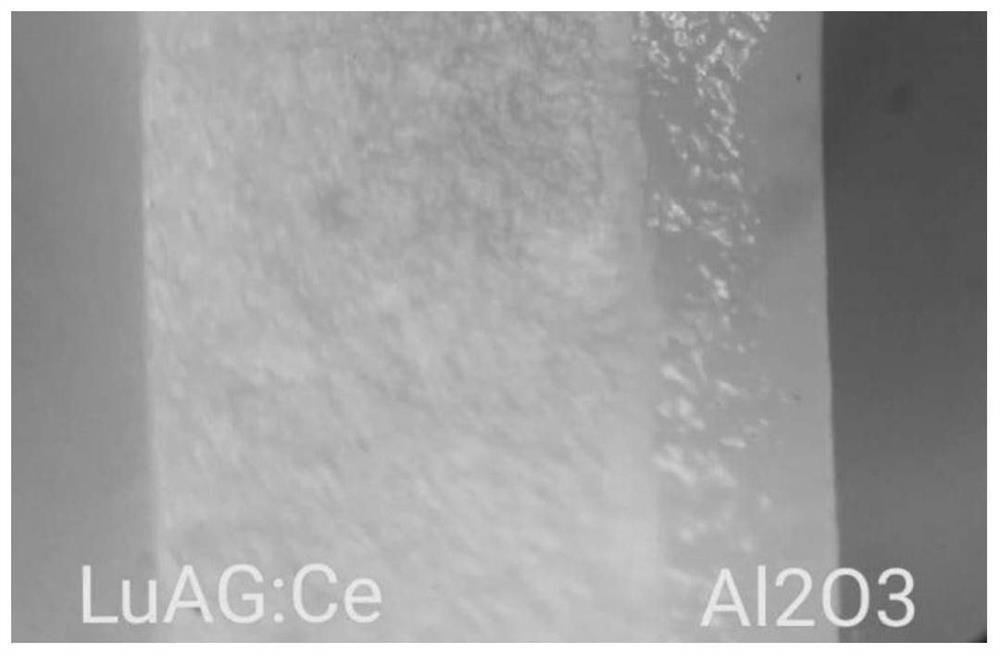
[0096] Step 3: Fabricate YAG:Ce, Mn-containing fluorescent transparent ceramic layer 2 and alumina ceramic bonding layer 3 with the same size as the chip wafer by casting method (see figure 1 ), the aluminum oxide transparent ceramic bonding layer and the light-emitting surface of the sapphire single crystal substrate are both Al 2 o 3 Materials, combined with the thermal bonding method of forming a covalent Al-O layer, the thermal bonding temperature is about 1300 ° C, at this time, the white LED chip is the LED chip wafer and the inorganic packaging material layer from bottom to top (see figure 2 ).
[0097] Step 4: Cutting the above-mentioned white light LED chip wafer packaged...
Embodiment 2
[0100] Step 1: Make a YAG:Ce fluorescent transparent ceramic sheet of a certain size, which is combined with a sapphire single crystal substrate by a metal bonding method of gold Au single layer, and the temperature of the metal bonding is 700°C.
[0101] Step 2: using the other side of the sapphire single crystal substrate as a substrate to grow an epitaxial structure, including a P-type epitaxial layer, an N-type epitaxial layer, and a light-emitting layer.
[0102] Step 3: On the epitaxial structure, a wafer with a flip-chip structure containing multiple LED chips is fabricated. At this time, the white LED chips are LED chip wafers and fluorescent transparent ceramic sheets from bottom to top.
[0103] Step 5: Cutting the above-mentioned white light LED chip wafer packaged with inorganic materials to form a flip-chip LED chip wafer with the required number of chips, and then package it with a conductive substrate COB to obtain a white light LED device.
[0104] The LED devi...
Embodiment 3
[0106] Step 1: growing an epitaxial structure based on a sapphire single crystal substrate, including an N-type epitaxial layer, a light-emitting layer, and a P-type epitaxial layer.
[0107] Step 2: Fabricate a flip-chip wafer containing multiple LED chips on the epitaxial structure.
[0108] Step 3: Make a fluorescent transparent ceramic bonding layer containing LuAG:Ce with the same size as the chip wafer, and adopt a silver-Ag single-layer metal bonding method, and the metal bonding temperature is 600°C.
[0109] Step 4: Cutting the above-mentioned white light LED chip wafer packaged with inorganic materials to form a flip-chip LED chip wafer with the required number of chips, and then package it with a conductive substrate COB to obtain a white light LED device.
[0110] The LED device of the above embodiment is tested by an integrating sphere system, and the luminous efficiency of the light source exceeds 195lm / W. Compared with the traditional flip chip disclosed in CN20...
PUM
| Property | Measurement | Unit |
|---|---|---|
| thickness | aaaaa | aaaaa |
| thickness | aaaaa | aaaaa |
| thickness | aaaaa | aaaaa |
Abstract
Description
Claims
Application Information
 - R&D
- Intellectual Property
- Life Sciences
- Materials
- Tech Scout
- Unparalleled Data Quality
- Higher Quality Content
- 60% Fewer Hallucinations
Browse by: Latest US Patents, China's latest patents, Technical Efficacy Thesaurus, Application Domain, Technology Topic, Popular Technical Reports.
© 2025 PatSnap. All rights reserved.Legal|Privacy policy|Modern Slavery Act Transparency Statement|Sitemap|About US| Contact US: help@patsnap.com