Heterogeneous integration method for monocrystalline two-dimensional semiconductor molybdenum telluride film and arbitrary lattice mismatched monocrystalline substrate

A two-dimensional semiconductor and lattice-mismatching technology, which is applied in semiconductor devices, semiconductor/solid-state device manufacturing, sustainable manufacturing/processing, etc., can solve problems that hinder the development of related devices, complex processes, and high cost of buffer layer technology

Pending Publication Date: 2022-04-19
PEKING UNIV
View PDF0 Cites 1 Cited by
  • Summary
  • Abstract
  • Description
  • Claims
  • Application Information

AI Technical Summary

Problems solved by technology

However, the integration of different kinds of single crystal materials in the same chip by heteroepitaxy is limited by lattice matching, and only two kinds of single crystal materials with similar lattice structures and lattice constants can be epitaxially grown, or on the substrate A buffer layer is added between the epitaxial layer to achieve heterogeneous integration, but the cost of the buffer layer technology is high and the process is complicated
Therefore, the limitation of lattice matching prevents the integration of many single crystal materials through heteroepitaxy, which hinders the development of related devices.

Method used


Image

  • Heterogeneous integration method for monocrystalline two-dimensional semiconductor molybdenum telluride film and arbitrary lattice mismatched monocrystalline substrate
  • Heterogeneous integration method for monocrystalline two-dimensional semiconductor molybdenum telluride film and arbitrary lattice mismatched monocrystalline substrate
  • Heterogeneous integration method for monocrystalline two-dimensional semiconductor molybdenum telluride film and arbitrary lattice mismatched monocrystalline substrate

Examples


Embodiment Construction

[0023] The present invention will be further elaborated below through specific embodiments in conjunction with the accompanying drawings.

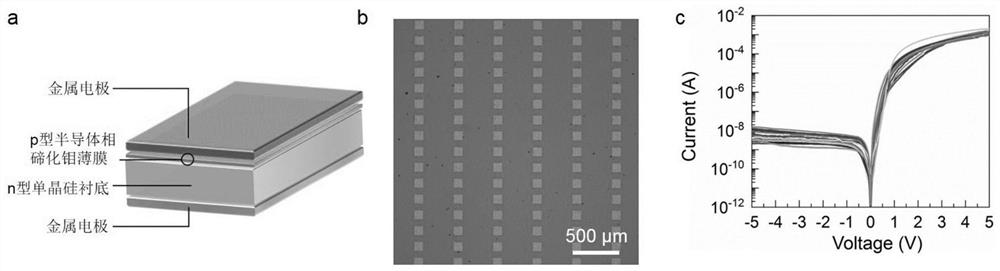
[0024] In this example, a pn junction device that is heterogeneously integrated with a two-dimensional semiconductor molybdenum telluride thin film and a variety of lattice-mismatched three-dimensional single crystal materials is prepared through the following steps:

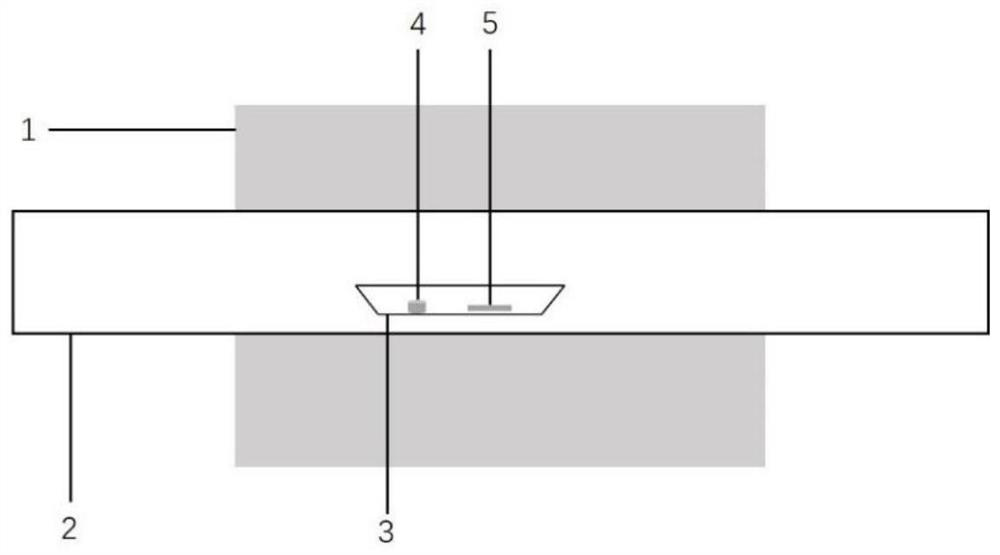
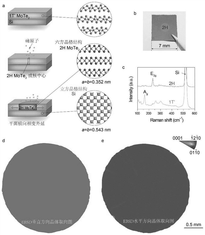
[0025] (1) Three-dimensional single-crystal substrate material preparation. In order to demonstrate the advantage that two-dimensional single-crystal semiconductor molybdenum telluride thin films can be directly grown on single-crystal materials with mismatched lattice structures, we selected molybdenum telluride thin films (hexagonal lattice structure) Different single crystal silicon materials are used as substrates (cubic lattice structure), and the crystal plane is [001]. The lattice constant of semiconductor molybdenum telluride is a=b=0.352nm, the lattice constant of s...


PUM

PropertyMeasurementUnit
thicknessaaaaaaaaaa
diameteraaaaaaaaaa

Abstract

The invention discloses a method for heterogeneous integration of a monocrystal two-dimensional semiconductor molybdenum telluride film and an arbitrary lattice mismatched monocrystal substrate. According to the method, the necessary condition, namely lattice matching, of heterogeneous integration of different types of single crystal materials in the traditional epitaxial process is broken through, and the 2H-MoTe2 prepared by utilizing the chemical vapor deposition method has a special growth mechanism of transverse epitaxial phase change; the monocrystal two-dimensional semiconductor molybdenum telluride film can be directly grown and integrated with any monocrystal substrate by controlling the temperature and the time without being limited by lattice matching. According to the obtained heterogeneous integrated structure, the semiconductor characteristic of molybdenum telluride and the physical characteristic of the substrate can be utilized at the same time, the performance of the device is improved, and the functionalization of the device is enhanced. Moreover, the method is suitable for large-area preparation, the preparation of an integrated photoelectric device array can be realized, a basis is provided for realizing wafer-level and industrial chip manufacturing, and a basis is provided for the application of a two-dimensional semiconductor material in the aspects of integrated circuits and photoelectric chips.

Description

technical field [0001] The invention relates to the field of semiconductors, in particular to a method for preparing a two-dimensional semiconductor material film by large-area epitaxy on a single crystal substrate with a variety of highly mismatched lattice structures. Background technique [0002] In order to expand the functions of chips or improve their performance in the semiconductor industry and related research fields, it is necessary to heterogeneously integrate high-quality single crystal materials with different physical properties into chips. Epitaxy, as a mature high-quality crystal growth method, has been developed for many semiconductors and is widely used in the fabrication of silicon-based semiconductors, such as bipolar heterojunction transistors and advanced complementary metal-oxide semiconductors (CMOS) . Epitaxy is also particularly important for compound semiconductors, such as the realization of a two-dimensional electron gas (2DEG) in gallium arseni...

Claims


Application Information

Patent Timeline
Patent Type & Authority Applications(China)
IPC IPC(8): H01L31/18H01L21/02H01L31/032H01L31/109
CPCH01L31/18H01L31/109H01L31/032H01L21/02381H01L21/02568H01L21/0262Y02P70/50
Inventor 潘宇徐晓龙李艳平叶堉
Owner PEKING UNIV
Why Eureka
Try Eureka