
Preparation method of low-loss silicon nitride waveguide

A silicon nitride, low-loss technology, used in the structure of optical waveguide semiconductors, semiconductor lasers, electrical components, etc., can solve the problems of introducing large sidewall roughness, increased loss, loss, etc., to avoid etching and direct Grinding, waveguide loss reduction, loss avoidance effect

Pending Publication Date: 2022-04-26
BEIJING CHANGCHENG INST OF METROLOGY & MEASUREMENT AVIATION IND CORP OF CHINA
View PDF8 Cites 0 Cited by
  • Summary
  • Abstract
  • Description
  • Claims
  • Application Information

AI Technical Summary

Problems solved by technology

[0003] Nevertheless, the existing silicon nitride waveguide method still has three disadvantages: first, due to its material characteristics, the loss of light to silicon nitride is higher than that of silicon oxide materials; secondly, the traditional silicon nitride waveguide processing method steps , the silicon nitride core layer will be etched by an etching method, which will introduce a large sidewall roughness, resulting in increased loss; third, most of the existing silicon nitride waveguides are at 300nm–500nm, not only because The problem of stress affects processing, and at the same time, thicker silicon nitride waveguides are more susceptible to sidewall roughness, resulting in greater losses

Method used


Image

  • Preparation method of low-loss silicon nitride waveguide
  • Preparation method of low-loss silicon nitride waveguide
  • Preparation method of low-loss silicon nitride waveguide

Examples


Embodiment 1

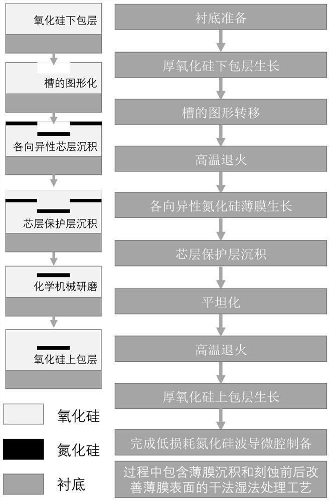
[0034] Such as figure 1 with figure 2 As shown, a method for preparing a low-loss silicon nitride waveguide disclosed in this embodiment includes:

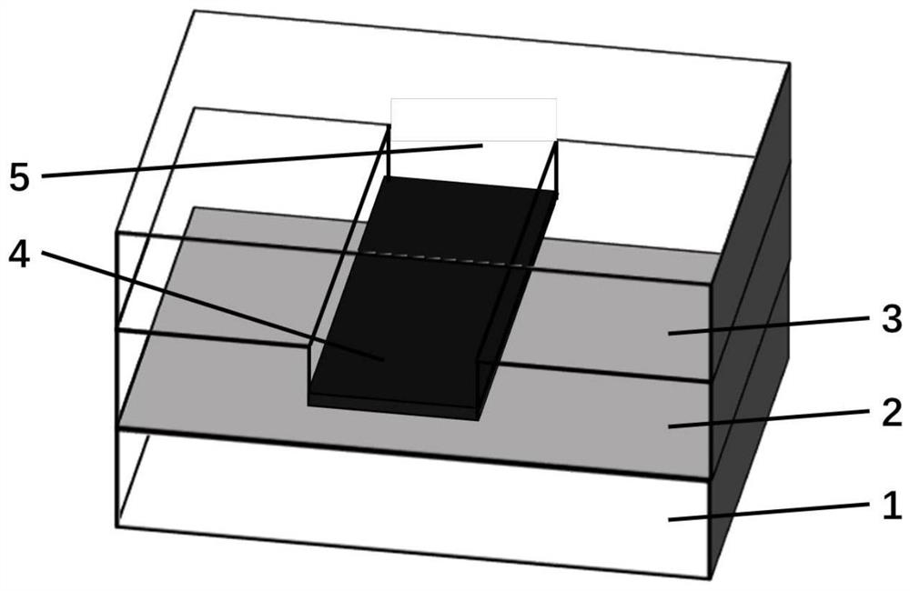
[0035] Step 1, first prepare the substrate, corresponding to figure 2 Substrate 1, cleaning the substrate before the furnace. Step 2, grow a 15 μm silicon oxide film on the substrate, using the wet oxygen oxidation method, corresponding to figure 2 SiO lower cladding 2. Step 3, use the designed layout to carry out the photolithographic etching method of the waveguide structure, complete the pattern transfer, and form the groove required to define the waveguide. The groove depth is 500nm, corresponding to figure 2 Groove 5 defining the waveguide. Step 4, perform high temperature annealing at about 1200° C. for 3 hours. In step 5, the anisotropic growth of the silicon nitride core film is carried out by using the HDPCVD method with substrate bias. The thickness of the core layer is 110 nm. The silicon nitride with thinne...


PUM


Abstract

The invention discloses a preparation method of a low-loss silicon nitride waveguide, and belongs to the technical field of silicon-based photonic device preparation. According to the invention, a thick silicon dioxide film is grown on a silicon wafer as a lower cladding; pattern transfer of a target waveguide groove is realized on the lower cladding through photoetching; performing high-temperature annealing to realize silicon dioxide reflux; depositing a silicon nitride film by using an anisotropic deposition method; growing a core layer protective layer silicon oxide film by using chemical vapor deposition; chemical mechanical planarization is used to remove the silicon nitride film at a high position, and silicon nitride in a groove is used as a waveguide core layer; performing high-temperature annealing to improve the morphology and optical loss of the silicon nitride; growing a thick silicon dioxide film as an upper cladding; and completing the preparation of the low-loss silicon nitride waveguide. According to the method, a method compatible with a CMOS platform is used, anisotropic groove filling and chemical mechanical grinding methods are utilized, etching and direct grinding of the waveguide core layer are avoided, and therefore loss caused by the surface roughness and damage of the core layer is avoided.

Description

technical field [0001] The invention relates to a method for preparing a low-loss silicon nitride waveguide, belonging to the technical field of silicon-based photonic device preparation. Background technique [0002] The silicon nitride material has a higher refractive index than silicon dioxide, and the thin-film approach to silicon oxide and silicon nitride is compatible with CMOS platforms. On a silicon-based platform, silicon nitride is an ideal core material; while silicon oxide has good photoelectric properties and extremely low optical loss, making it the best choice for cladding materials. Today, with the rapid development of silicon-based photonics, low-loss waveguides, microcavities, gratings and other structures with silicon nitride as the core layer can provide huge method and technical support for photonics design. [0003] Nevertheless, the existing silicon nitride waveguide method still has three disadvantages: first, due to its material characteristics, the...

Claims


Application Information

Patent Timeline
Patent Type & Authority Applications(China)
IPC IPC(8): H01S5/22
CPCH01S5/22H01S5/2202
Inventor 李昱东李维冯梁森李小宽刘雅丽
Owner BEIJING CHANGCHENG INST OF METROLOGY & MEASUREMENT AVIATION IND CORP OF CHINA
Learn More