
A manufacturing method of a composite sensor package carrier board and a lidar sensor

A technology for packaging a carrier board and a manufacturing method, which is applied in the directions of printed circuit manufacturing, instruments, circuit optical components, etc., can solve the problems of inability to carry out complex and precise circuits, high cost, and difficult processing, and achieves improved miniaturization and integration. Good air tightness and reliability, and the effect of reducing production costs

Active Publication Date: 2022-07-12
东莞市春瑞电子科技有限公司
View PDF0 Cites 0 Cited by
  • Summary
  • Abstract
  • Description
  • Claims
  • Application Information

AI Technical Summary

Problems solved by technology

[0002] At present, the package of consumer electronic sensors such as mobile phones is usually packaged with a flat PCB substrate. First, the chip is packaged on the PCB substrate, and then sealed with die-casting plastic sealant. Finally, a single device is formed by injecting a shielding protective plastic shell. Plastic and injection-molded shielding protection plastic shells have high requirements, the yield of finished products is low, and the cost is high, and the packaged finished devices still have quality problems such as air tightness, sensitivity, and stability.
[0003] The high-performance solid-state lidar sensor package usually uses a ceramic substrate as the package carrier. Although it has the advantages of good sealing, high stability, and good heat dissipation performance, the ceramic substrate is brittle and fragile, and the adhesion of the surface metal circuit Poor, difficult to perform complex and precise processing and other shortcomings, resulting in bulky dimensions of the finished sensor device, and the inability to process complex and precise circuits, it is difficult to meet the packaging requirements of higher-performance chips, and the size or performance of the packaged lidar sensor device is limited. In addition, the ceramic substrate is fragile, and the number of holes cannot be drilled too much, which makes the processing difficult;
[0004] In addition, the solid-state lidar sensor packaging ceramic substrate basically relies on imported or directly imported finished devices, and the price is very high, especially the optical phased array (OPA) all-solid-state lidar sensor, which is currently only monopolized by large foreign companies. For example, Quanergy Corporation of the United States recently launched a laser radar sensor based on solid-state OPA technology; for automatic driving and other requirements, it has a high-performance laser radar sensor with ultra-long detection distance, high precision, high sensitivity, high reliability, high integration and miniaturization. There is a problem of being stuck in the country, and due to the basic characteristics of the ceramic substrate, it also hinders the lidar sensor from better meeting the higher needs of the development of autonomous driving

Method used


Image

  • A manufacturing method of a composite sensor package carrier board and a lidar sensor
  • A manufacturing method of a composite sensor package carrier board and a lidar sensor
  • A manufacturing method of a composite sensor package carrier board and a lidar sensor

Examples


Embodiment 1

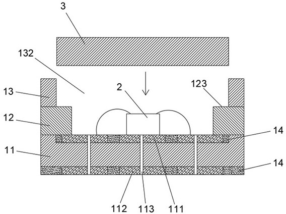
[0034] Embodiment 1, refer to figure 2 ;

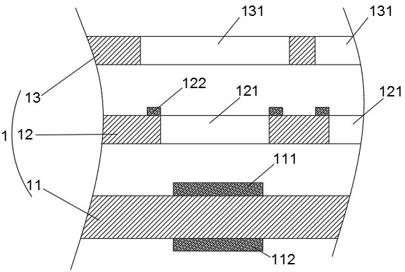
[0035] In the first step, a preset through hole 113 is formed through the PCB circuit substrate 11 by means of mechanical or laser drilling, and then a conductive layer is formed in the through hole 113 by electroplating or filling metal material; Steps such as etching form a functional circuit on the PCB circuit substrate 11, and two sides of the functional circuit are respectively formed with a package pad 1 111 and a package pad 2 112, and a conductive connection is formed through a preset through hole 2 113;

[0036] In the second step, the PCB circuit substrate 11 , the first optical cup board 12 and the second optical cup board 13 are stacked and pressed together to form the package carrier board 1 by vacuum thermocompression bonding with epoxy resin glue. First press the PCB circuit substrate 11 and the first optical cup board 12, and then press the second optical cup board 13 on the first optical cup board 12, or the PCB cir...

Embodiment 2

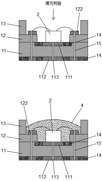
[0049] Embodiment 2, refer to image 3 ;

[0050] The traditional sensor bonding method requires at least two bonding pads on the package carrier 1, one for die bonding (fixed chip) and the other for bonding bonding wires; The requirements for precision, sensitivity and function of components are getting higher and higher, and the packaging chip circuits used are more complex, which means that more and denser bonding pads are required for connecting bonding wires, which limits the packaging carrier board 1 further miniaturization.

[0051] In view of the above-mentioned problems, the following processing steps are added before and after the second step in the first embodiment:

[0052] Before the second step, the side of the first optical cup board 12 away from the PCB circuit substrate 11 is covered with copper foil, and the first optical cup board 12 and the PCB circuit substrate 11 are covered with epoxy resin glue, so that the packaging of the PCB circuit substrate 11 is...

Embodiment approach

[0055] The present invention also provides a lidar sensor, comprising the above-mentioned package carrier board 1 , a package pad 1 111 in the package carrier board 1 is bonded with a functional chip 2 , and a mounting position 132 located above the functional chip 2 is fixed with a Optical unit, according to the above two embodiments, the lidar sensor also has various implementations, as follows:

[0056] In the first embodiment, the functional chip 2 and the bonding wire are both bonded to the package pad 1 111 located in the first optical cup hole 121, and the optical unit is the optical filter 3, which is installed in the installation position 132. The solution is: It is formed on the basis of the first embodiment, and the technical effect brought by it is the same, and the specific content can refer to the description in the first embodiment;

[0057] In the second embodiment, the functional chip 2 and the bonding wire are both bonded to the package pad one 111 located in...


PUM


Abstract

The invention discloses a manufacturing method of a composite sensor package carrier board and a laser radar sensor, comprising a PCB circuit substrate, a first optical cup board, and a second optical cup board. A functional circuit is formed on it, and the packaging pad 1 and the packaging pad 2 are made; the second step is to insert the solder resist material on the PCB circuit substrate, and the window is opened; the third step, the PCB circuit substrate, the first light The cup board and the second optical cup board are stacked and pressed together by vacuum thermocompression to form a carrier board profile with a plurality of packaging carrier boards, and the second optical cup board and the first optical cup board are pressed together on one of the packaging pads. The installation position with steps is formed above; the fourth step is to divide the carrier plate profile into suitable sizes according to the actual situation. The setting of the installation position can effectively limit the position of the optical unit and avoid the process of thermal pressing. Middle sliding shift.

Description

technical field [0001] The invention belongs to the technical field of chip packaging, in particular to a manufacturing method of a composite sensor packaging carrier board and a laser radar sensor. Background technique [0002] At present, the packaging of consumer electronic sensors such as mobile phones is usually packaged with a flat PCB substrate. First, the chip is packaged on the PCB substrate, then die-casting plastic sealant is sealed, and finally the shielding and protective plastic shell is injection-molded to form a single device. The manufacturing process is complex, and the die-casting plastic packaging Glue and injection-molded shielding have high requirements for protecting plastic housings, resulting in low yield and high cost of finished products. Moreover, the packaged finished devices still have quality problems such as air tightness, sensitivity, and stability. [0003] The high-performance solid-state lidar sensor package usually uses a ceramic substrat...

Claims


Application Information

Patent Timeline
Patent Type & Authority Patents(China)
IPC IPC(8): H05K3/40H05K1/02H05K1/18H05K3/00H05K3/36G01S7/481
CPCH05K3/4007H05K3/368H05K3/0052H05K1/181H05K1/0274G01S7/481
Inventor 周志国钟峰
Owner 东莞市春瑞电子科技有限公司
Learn More